

3D Semiconductor Packaging Market Report 2026
Global Outlook – By Type ( 3D Through Silicon Via, 3D Package On Package, 3D Fan Out Based, 3D Wire Bonded), By Material ( Organic Substrate, Bonding Wire, Leadframe, Encapsulation, Resins, Ceramic Packages, Die Attach Material, Other Materials), By Industry ( Electronics, Industrial, Automotive And Transport, Healthcare, IT And Telecommunication Or Aerospace And Defense) – Market Size, Trends, Strategies, and Forecast to 2030
3D Semiconductor Packaging Market Overview
• 3D Semiconductor Packaging market size has reached to $18.02 billion in 2025 • Expected to grow to $36.06 billion in 2030 at a compound annual growth rate (CAGR) of 14.8% • Growth Driver: 3D Semiconductor Packaging Market To Grow As Functionality And Applications Expand • Market Trend: Technological Advancements Driving Innovation In 3D Semiconductor Packaging • Asia-Pacific was the largest region in 2025.Market Gains By 2030 – Top Opportunities By Segment
Market Gain identifies the most promising market opportunities by highlighting the segments or products expected to generate the highest incremental revenue growth over the next five years.
What Is Covered Under 3D Semiconductor Packaging Market?
3D semiconductor packaging refers to 3D integration systems that achieve vertical stacking through standard interconnection methods such as wire bonding and flip chips. It is used to improve the performance of electrical devices that operate at high frequencies. The main types of 3D semiconductor packaging are 3D through silicon via, 3D package on package, 3D fan out based, and 3D wire bonded. 3D through silicon refers to the type of via (vertical interconnect access) connection used in microchip engineering and manufacturing that completely passes through a silicon die or wafer to allow for stacking of silicon dice. The materials used are organic substrate, bonding wire, lead frame, encapsulation, resins, ceramic packages, die to attach materials and others that are used in various industries such as electronics, industrial, automotive and transport, healthcare, IT, telecommunication and aerospace and defense industry.
What Is The 3D Semiconductor Packaging Market Size 2026 And Growth Rate?
The 3D semiconductor packaging market size has grown rapidly in recent years. It will grow from $18.02 billion in 2025 to $20.75 billion in 2026 at a compound annual growth rate (CAGR) of 15.2%. The growth in the historic period can be attributed to growth in conventional 2d packaging, early adoption of wire bonding integration, expansion in computing and telecommunications, growth in memory packaging applications, reliance on outsourced semiconductor packaging.What Is The 3D Semiconductor Packaging Market Growth Forecast?
The 3D semiconductor packaging market size is expected to see rapid growth in the next few years. It will grow to $36.06 billion in 2030 at a compound annual growth rate (CAGR) of 14.8%. The growth in the forecast period can be attributed to increasing demand for high-performance computing chips, rising adoption of heterogeneous integration, expansion of advanced system-in-package solutions, development of low-power high-density architectures, rising deployment in automotive electronics. Major trends in the forecast period include development of AI-optimized chip stacking architectures, expansion of high-density vertical integration platforms, adoption of smart automated packaging systems, advancement of IoT-enabled semiconductor manufacturing, integration of autonomous inspection and testing systems.

Global 3D Semiconductor Packaging Market Segmentation
1) By Type: 3D Through Silicon Via, 3D Package On Package, 3D Fan Out Based, 3D Wire Bonded 2) By Material: Organic Substrate, Bonding Wire, Leadframe, Encapsulation, Resins, Ceramic Packages, Die Attach Material, Other Materials 3) By Industry: Electronics, Industrial, Automotive And Transport, Healthcare, IT And Telecommunication Or Aerospace And Defense Subsegments: 1) By 3D Through Silicon Via (TSV): Wafer-Level Packaging, System-In-Package (SiP), 3D Package On Package (PoP), Memory PoP, Logic PoP 2) By 3D Fan Out Based: Molded Fan-Out (MFO), Wafer Fan-Out (WFO) 3) By 3D Wire Bonded: Standard Wire Bonding, Advanced Wire Bonding Techniques The top segments in the 3d semiconductor packaging market will be: • Organic Substrate will reach $14075.87 Million by 2030. • 3D Through Silicon Via (TSV) will reach $13033.09 Million by 2030. • Electronics will reach $12079.94 Million by 2030. • 3D Package On Package (PoP) will reach $10348.43 Million by 2030. • 3D Fan Out Based will reach $8237.49 Million by 2030.What Is The Driver Of The 3D Semiconductor Packaging Market?
Increasing the functionality and application scope of semiconductor or IC packages is expected to propel the growth of the 3D semiconductor packaging market going forward. A semiconductor is a solid substance with conductivities between an insulator and a conductor. The IC packaging is a common method for boosting integration density and performance in a single package. For instance, in July 2024, according to the Bureau of Labor Statistics, a US-based government agency In 2023, the total trade value of exported semiconductors reached $65.9 billion, reflecting a 12.5% decline compared to 2022. The top six exporting states accounted for 71.0% of the overall trade value. Therefore, increasing the functionality and application scope of semiconductor or IC packages is driving the 3D semiconductor packaging industry.
Infographic Chart Showing Key Market Drivers Analysis And Restraints For 3D Semiconductor Packaging Market
The chart presents an impact analysis of key drivers and restraints, quantifying their relative influence on the market's growth rate and helping assess the balance between growth enablers and limiting factors. This chart offers a high-level perspective; the full report contains more detailed insights.
How Will The Drivers Impact Growth In The Global 3D Semiconductor Packaging Market?
• Growing Need For Miniaturized Components (High) – During the forecast period, the growing need for miniaturized components is driving increased demand for 3d semiconductor packaging. as electronic devices, advanced computing systems, and consumer electronics continue to demand smaller, faster, and more energy-efficient components, manufacturers increasingly focus on reducing the size of chips and interconnects without compromising performance. the growing integration of micro-scale components, high-density circuits, and compact interconnects enables higher functionality within limited spaces while improving thermal management and power efficiency. the increasing reliance on miniaturized components to enhance device performance, reduce footprint, and support complex system designs is driving demand for innovative 3d semiconductor packaging solutions that can efficiently accommodate smaller, high-performance, and highly integrated electronic systems. as miniaturization continues to transform electronics and semiconductor technologies, the 3d semiconductor packaging market is expected to witness significant growth, driven by the need for compact, efficient, and high-performance packaging solutions. the growing need for miniaturized components growth contribution during the forecast period in 2025 is 2.0%. • Increasing Semiconductor Manufacturing Investments And Government Incentive (Medium) – During the forecast period, the increasing semiconductor manufacturing investments and supportive government incentive programs is driving demand for 3d semiconductor packaging. as countries focus on strengthening domestic semiconductor supply chains and reducing dependence on imports, governments and private sector players are committing significant capital toward establishing fabrication plants, assembly, testing, and packaging facilities. large-scale initiatives such as national semiconductor missions, production-linked incentives, and capital subsidies are encouraging the expansion of semiconductor manufacturing ecosystems across multiple regions. these investments are also supporting the development of advanced packaging infrastructure, including facilities focused on assembly, testing, and packaging operations that are essential for modern chip production. the rising number of semiconductor manufacturing projects and supportive fiscal policies aimed at boosting chip production are increasing demand for advanced packaging technologies, thereby accelerating growth in the 3d semiconductor packaging market during the forecast period. the increasing semiconductor manufacturing investments and supportive government incentive programs growth contribution during the forecast period in 2025 is 1.5%. • Increasing High-Performance Computing Demand (Medium) – During the forecast period, increasing high-performance computing demand are accelerating the adoption of 3d semiconductor packaging. as industries increasingly rely on data-intensive applications such as artificial intelligence, cloud computing, and large-scale data analytics, the need for advanced computing infrastructure capable of processing massive workloads is rising significantly. the growing adoption of hpc systems requires semiconductor architectures that can deliver higher processing speeds, improved bandwidth, and enhanced energy efficiency. 3d semiconductor packaging enables the integration of multiple chips and high-bandwidth memory within a compact structure, improving data transfer rates and reducing latency between components. the expanding demand for high-performance computing solutions across data centers, research institutions, and enterprise applications is therefore accelerating the adoption of advanced packaging technologies and driving growth in the 3d semiconductor packaging market. the increasing high-performance computing demand growth contribution during the forecast period in 2025 is 1.0%. • Rising 5G infrastructure Deployment (Low) – During the forecast period, the rising 5g infrastructure deployment is accelerating the adoption of 3d semiconductor packaging. as telecom operators and governments continue expanding next-generation wireless networks globally, the demand for high-performance semiconductor devices capable of supporting advanced connectivity and data processing is also increasing. the rapid rollout of 5g networks requires sophisticated chips with higher bandwidth, lower latency, and improved power efficiency, which are increasingly enabled through advanced packaging solutions such as 3d semiconductor packaging. furthermore, the growing adoption of 5g-enabled services, including fixed wireless access and high-speed broadband connectivity, is accelerating demand for advanced semiconductor components. according to industry reports, global 5g subscriptions are projected to reach approximately 2.9 billion by 2025, highlighting the scale of ongoing network expansion. the increasing deployment of 5g infrastructure and the rising demand for high-performance semiconductor solutions are therefore driving growth in the 3d semiconductor packaging market. the rising 5g infrastructure deployment growth contribution during the forecast period in 2025 is 0.5%.How Will The Restraints Impact Growth In The Global 3D Semiconductor Packaging Market?
• Complex Testing And Quality Assurance Requirements (High) – During the forecast period, the increasing complexity of testing and quality assurance requirements limits a significant barrier to market expansion. as semiconductor designs become more intricate and manufacturing processes advance, the demand for rigorous quality control and testing protocols is rising globally. the need for specialized testing frameworks, automated inspection tools, and ai-powered quality assurance solutions ensures that packaging integrity, thermal performance, and electrical reliability meet stringent industry standards. the growing emphasis on minimizing defects, ensuring device reliability, and adhering to industry compliance is driving demand for advanced testing and quality assurance solutions in the 3d semiconductor packaging market. growth affected by increasing complexity of testing and quality assurance requirements during the forecast period in 2025 is -1.5%. • Thermal Management And Heat Dissipation Constraints (Medium) – During the forecast period, the thermal management and heat dissipation constraints remains a significant barrier to market expansion. as device performance continues to increase and die stacking becomes more complex, localized heat accumulation and high-power density in vertically integrated chips are creating significant thermal challenges. inefficient heat spreading through multiple layers, interfaces, and materials can limit operating frequency, accelerate aging, and reduce overall reliability. the rising need for effective thermal design strategies, including optimized stack organization, interface materials, and cooling solutions, is driving demand for advanced 3d semiconductor packaging solutions that ensure performance, yield, and system longevity. growth affected by thermal management and heat dissipation constraints during the forecast period in 2025 is -1.0%. • Trade War And Tariffs (Medium) – During the forecast period, the trade war and tariffs remains a significant barrier to market expansion. as geopolitical tensions and protectionist policies continue to rise globally, restrictions on critical raw materials and semiconductor components are increasingly affecting the supply chain. the growing presence of tariffs and trade barriers disrupts access to essential inputs such as rare earth elements, which are vital for advanced semiconductor manufacturing. the increasing focus on domestic sourcing and investment in alternative supply chains to mitigate trade risks is driving demand for advanced 3d semiconductor packaging solutions. the rising need to maintain production continuity, ensure supply chain resilience, and support high-performance chip manufacturing is expected to propel 3d semiconductor packaging market growth in the coming years. growth affected by trade war and tariffs during the forecast period in 2025 is -0.3%.Key Players In The Global 3D Semiconductor Packaging Market
Major companies operating in the 3D semiconductor packaging market are Amkor Technology Inc., Advanced Semiconductor Engineering Inc., International Business Machines Corporation, Jiangsu Changjiang Electronics Technology Co. Ltd., Qualcomm Technologies Inc., Samsung Electronics Corporation Ltd., Siliconware Precision Industries Co. Ltd., STMicroelectronics NV, SÜSS MICROTEC SE, Taiwan Semiconductor Manufacturing Company Limited, 3M Company, Advanced Micro Devices Inc., Walton Advanced Engineering Inc., China Wafer Level CSP Co. Ltd., Chipbond Technology Corporation, Chipmos Technologies Inc., Lingsen Precision Industries Ltd., Micron Technology Inc., Powertech Technology Inc., Tokyo Electron Ltd., Toshiba Corporation, Unisem, United Microelectronics Corporation, United Test and Assembly Center Ltd., ON Semiconductor, Renesas Electronics Corporation, Skyworks Solutions Inc., Analog Devices, Inc., Broadcom Inc., Cypress Semiconductor Corporation, Maxim Integrated, Microchip Technology Inc., Texas Instruments Incorporated
This chart is for illustrative purposes; the full report includes a detailed competitor analysis and comprehensive overview of the top 10 companies in the market.

This chart maps companies by product innovation and brand strength, with bubble size indicating relative revenue, helping identify market leaders, challengers, and niche players. This is an illustrative chart; the full report provides a complete and accurate competitive analysis.
Global 3D Semiconductor Packaging Market Trends and Insights
Major companies entering the semiconductor packaging market are adopting technological innovations such as 3D stacking techniques for semiconductor packaging to reduce the cost of production and customize products to attract clients. For instance, in January 2023, Canon, a US-based company, launched a semiconductor lithography i-line stepper system for 3D packaging technologies. This system has a resolution of 0.8 µm and is designed to support the latest packaging trends. It provides cost-effective imaging for the front and back ends of the line. Canon's FPA-5520iV HR option for back-end i-line steppers achieves a resolution of 0.8 µm to cater to the evolving demands of the semiconductor industry. Furthermore, Canon's i-line steppers, such as the FPA-3030i5a and FPA-8000iW, can offer low-cost-of-ownership manufacturing for small substrates and advanced panel-level packaging (PLP) applications, respectively.What Are Latest Mergers And Acquisitions In The 3D Semiconductor Packaging Market?
In April 2024, SK hynix Inc., a South Korea-based semiconductor manufacturer, partnered with Taiwan Semiconductor Manufacturing Company Limited, to develop next-generation high bandwidth memory (HBM) and improve logic and HBM integration using advanced packaging technology. Following the acquisition, the companies plan to begin by boosting the efficiency of the base die located at the foundation of the High Bandwidth Memory (HBM) package. They will work together to refine the integration of SK hynix’s HBM with TSMC’s CoWoS2 technology and coordinate efforts to meet shared customer demands for HBM products. Taiwan Semiconductor Manufacturing Company Limited is a Taiwan-based company specializing in 3D semiconductor packaging.
Regional Outlook
Asia-Pacific was the largest region in the 3D semiconductor packaging market share in 2025. The regions covered in this market report are Asia-Pacific, South East Asia, Western Europe, Eastern Europe, North America, South America, Middle East, Africa. The countries covered in this market report are Australia, Brazil, China, France, Germany, India, Indonesia, Japan, Taiwan, Russia, South Korea, UK, USA, Canada, Italy, Spain.What Defines the 3D Semiconductor Packaging Market?
The 3D semiconductor packaging market consists of revenues earned by entities by providing automation system services, integrated turnkey services, and interconnection and termination technology services. The market value includes the value of related goods sold by the service provider or included within the service offering. The 3D semiconductor packaging market also includes sales of bonding and debonding machines. Values in this market are ‘factory gate’ values, that is the value of goods sold by the manufacturers or creators of the goods, whether to other entities (including downstream manufacturers, wholesalers, distributors, and retailers) or directly to end customers. The value of goods in this market includes related services sold by the creators of the goods.How is Market Value Defined and Measured?
The market value is defined as the revenues that enterprises gain from the sale of goods and/or services within the specified market and geography through sales, grants, or donations in terms of the currency (in USD unless otherwise specified). The revenues for a specified geography are consumption values that are revenues generated by organizations in the specified geography within the market, irrespective of where they are produced. It does not include revenues from resales along the supply chain, either further along the supply chain or as part of other products.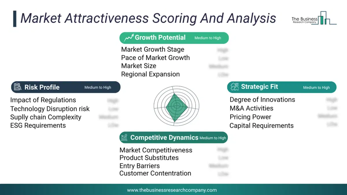
This chart presents market attractiveness based on a quantitative evaluation of growth, competition, strategic alignment, and risk, offering a clear view of opportunity areas for decision-making. This chart is for illustrative purposes; the full report contains the complete analysis.
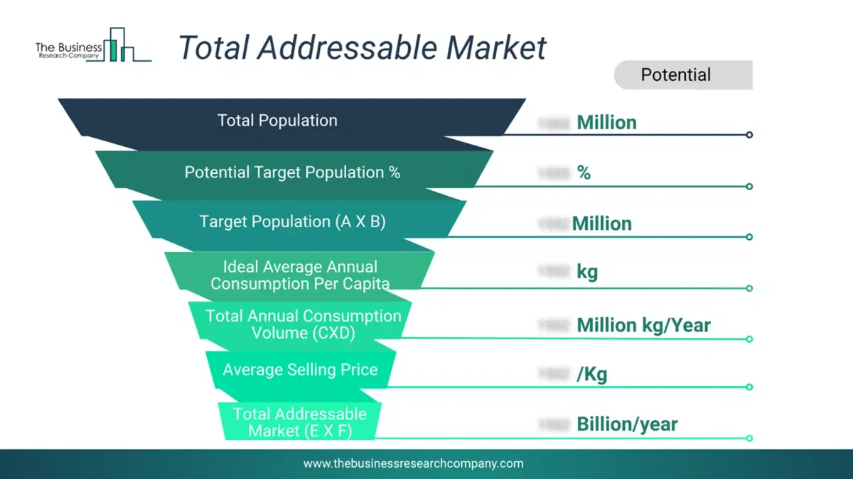
This chart highlights the Total Addressable Market (TAM) by estimating the maximum revenue opportunity using an assumption-driven approach, supporting strategic planning and opportunity sizing across markets. The chart is illustrative; the full report provides a more comprehensive analysis.
What Key Data and Analysis Are Included in the 3D Semiconductor Packaging Market Report 2026?
The 3d semiconductor packaging market research report is one of a series of new reports from The Business Research Company that provides market statistics, including industry global market size, regional shares, competitors with the market share, detailed market segments, market trends and opportunities, and any further data you may need to thrive in the 3d semiconductor packaging industry. The market research report delivers a complete perspective of everything you need, with an in-depth analysis of the current and future state of the industry.3D Semiconductor Packaging Market Report 2026 Market Report Forecast Analysis
| Report Attribute | Details |
|---|---|
| Market Size Value In 2026 | $20.75 billion |
| Revenue Forecast In 2030 | $36.06 billion |
| Growth Rate | CAGR of 15.2% from 2026 to 2030 |
| Base Year For Estimation | 2025 |
| Actual Estimates/Historical Data | 2020-2025 |
| Forecast Period | 2026 - 2030 - 2035 |
| Market Representation | Revenue in USD Billion and CAGR from 2026 to 2030 |
| Segments Covered | Type, Material, Industry |
| Regional Scope | Asia-Pacific, Western Europe, Eastern Europe, North America, South America, Middle East, Africa |
| Country Scope | The countries covered in the report are Australia, Brazil, China, France, Germany, India, Indonesia, Japan, Taiwan, Russia, South Korea, UK, USA, Canada, Italy, Spain. |
| Key Companies Profiled | Amkor Technology Inc., Advanced Semiconductor Engineering Inc., International Business Machines Corporation, Jiangsu Changjiang Electronics Technology Co. Ltd., Qualcomm Technologies Inc., Samsung Electronics Corporation Ltd., Siliconware Precision Industries Co. Ltd., STMicroelectronics NV, SÜSS MICROTEC SE, Taiwan Semiconductor Manufacturing Company Limited, 3M Company, Advanced Micro Devices Inc., Walton Advanced Engineering Inc., China Wafer Level CSP Co. Ltd., Chipbond Technology Corporation, Chipmos Technologies Inc., Lingsen Precision Industries Ltd., Micron Technology Inc., Powertech Technology Inc., Tokyo Electron Ltd., Toshiba Corporation, Unisem, United Microelectronics Corporation, United Test and Assembly Center Ltd., ON Semiconductor, Renesas Electronics Corporation, Skyworks Solutions Inc., Analog Devices, Inc., Broadcom Inc., Cypress Semiconductor Corporation, Maxim Integrated, Microchip Technology Inc., Texas Instruments Incorporated |
| Customization Scope | Request for Customization |
| Pricing And Purchase Options | Explore Purchase Options |