

Semiconductor And Integrated Circuit (IC) Packaging Materials Market Report 2026
Global Outlook – By Type (Organic Substrate, Bonding Wires, Leadframes, Encapsulation Resins, Ceramic Packages, Die Attach Materials, Solder Balls), By Packaging Technology (Small Outline Package, Grid Array, Quad Flat No Leads, Dual Flat No Leads, Quad Flat Packages, Dual In Line Package), By Application (Smartphones, Tablets And Laptops, Servers, Networking Equipment, Electric Vehicles, Autonomous Driving Systems, Industrial Automation Equipment), By End Use Industry (Consumer Electronics, Automotive, Healthcare, Information Technology And Telecommunication, Aerospace And Defense) – Market Size, Trends, Strategies, and Forecast to 2030
Semiconductor And Integrated Circuit (IC) Packaging Materials Market Overview
• Semiconductor And Integrated Circuit (IC) Packaging Materials market size has reached to $50.32 billion in 2025 • Expected to grow to $86.15 billion in 2030 at a compound annual growth rate (CAGR) of 11.3% • Growth Driver: Rising Demand For Consumer Electronics Devices Fueling The Growth Of The Market Due To Greater Digital Connectivity • Market Trend: Advanced 3.5D System-In-Package (SiP) Architecture Innovations Enhance Artificial Intelligence (AI) Chip Performance And Scalability • Asia-Pacific was the largest region in 2025 and North America is the fastest growing region.What Is Covered Under Semiconductor And Integrated Circuit (IC) Packaging Materials Market?
Semiconductor and integrated circuit (IC) packaging materials are specialized materials used to protect, support, connect, and enhance the performance of semiconductor devices and integrated circuits (ICs) after chip fabrication. They play a critical role in ensuring the reliability, durability, miniaturization, and functionality of semiconductor components. The main types of semiconductor and integrated circuit (IC) packaging materials include organic substrate, bonding wires, leadframes, encapsulation resins, ceramic packages, die attach materials, and solder balls. Organic substrate refers to an insulating base material that provides mechanical support and electrical interconnection between the semiconductor die and the printed circuit board in integrated circuit packaging. These materials are used with packaging technologies including small outline package, grid array, quad flat no leads, dual flat no leads, quad flat packages, and dual in line package. The various applications involved are smartphones, tablets and laptops, servers, networking equipment, electric vehicles, autonomous driving systems, and industrial automation equipment, and they are utilized by end-use industries including consumer electronics, automotive, healthcare, information technology and telecommunication, and aerospace and defense.
What Is The Semiconductor And Integrated Circuit (IC) Packaging Materials Market Size and Share 2026?
The semiconductor and integrated circuit (IC) packaging materials market size has grown rapidly in recent years. It will grow from $50.32 billion in 2025 to $56.2 billion in 2026 at a compound annual growth rate (CAGR) of 11.7%. The growth in the historic period can be attributed to increasing demand for consumer electronics devices, growing semiconductor manufacturing activities globally, rising adoption of advanced integrated circuits, expanding production of electronic components, increasing need for reliable semiconductor protection and connectivity solutions.What Is The Semiconductor And Integrated Circuit (IC) Packaging Materials Market Growth Forecast?
The semiconductor and integrated circuit (IC) packaging materials market size is expected to see rapid growth in the next few years. It will grow to $86.15 billion in 2030 at a compound annual growth rate (CAGR) of 11.3%. The growth in the forecast period can be attributed to increasing demand for advanced semiconductor packaging in high performance computing, rising adoption of electric vehicles and autonomous systems, growing requirement for miniaturized electronic components, expanding semiconductor fabrication capacity worldwide, increasing demand for high efficiency thermal management materials. Major trends in the forecast period include increasing adoption of advanced semiconductor packaging materials, growing demand for high performance ic packaging solutions, rising need for miniaturized and thermally efficient packaging materials, expanding use of advanced substrate and die attach materials, increasing development of high reliability semiconductor packaging technologies.

Global Semiconductor And Integrated Circuit (IC) Packaging Materials Market Segmentation
2) By Packaging Technology: Small Outline Package, Grid Array, Quad Flat No Leads, Dual Flat No Leads, Quad Flat Packages, Dual In Line Package 3) By Application: Smartphones, Tablets And Laptops, Servers, Networking Equipment, Electric Vehicles, Autonomous Driving Systems, Industrial Automation Equipment 4) By End Use Industry: Consumer Electronics, Automotive, Healthcare, Information Technology And Telecommunication, Aerospace And Defense Subsegments: 1) By Organic Substrate: Ajinomoto Build Up Film Substrate Type, Bismaleimide Triazine Resin Substrate Type, Flexible Organic Substrate Type, Rigid Organic Substrate Type, High Density Interconnect Substrate Type, Build Up Substrate Type 2) By Bonding Wires: Gold Bonding Wire Type, Copper Bonding Wire Type, Silver Bonding Wire Type, Palladium Coated Copper Wire Type, Aluminum Bonding Wire Type, Alloy Bonding Wire Type 3) By Leadframes: Copper Leadframe Type, Alloy Leadframe Type, Stamped Leadframe Type, Etched Leadframe Type, Multi Layer Leadframe Type, Fine Pitch Leadframe Type 4) By Encapsulation Resins: Epoxy Molding Compound Type, Liquid Encapsulation Resin Type, Silicone Encapsulation Resin Type, Ultraviolet Curable Encapsulation Resin Type, Thermosetting Encapsulation Resin Type, Low Stress Encapsulation Resin Type 5) By Ceramic Packages: Alumina Ceramic Package Type, Aluminum Nitride Ceramic Package Type, Low Temperature Co Fired Ceramic Package Type, High Temperature Co Fired Ceramic Package Type, Multilayer Ceramic Package Type, Hermetic Ceramic Package Type 6) By Die Attach Materials: Conductive Die Attach Material Type, Non Conductive Die Attach Material Type, Epoxy Die Attach Material Type, Silver Filled Die Attach Material Type, Solder Based Die Attach Material Type, Film Die Attach Material Type 7) By Solder Balls: Lead Free Solder Ball Type, Tin Silver Copper Solder Ball Type, Tin Copper Solder Ball Type, High Lead Solder Ball Type, Micro Solder Ball Type, Fine Pitch Solder Ball TypeWhat Is The Driver Of The Semiconductor And Integrated Circuit (IC) Packaging Materials Market?
The rising demand for consumer electronics devices is expected to propel the growth of the semiconductor and integrated circuit (IC) packaging materials market going forward. Consumer electronics devices are electronic products intended for everyday personal use, including smartphones, laptops, tablets, televisions, wearable devices, and smart home products. Consumer electronics devices are rising due to growing digital connectivity needs, as consumers increasingly depend on electronic devices for communication, entertainment, work, and everyday convenience. Semiconductor & IC packaging materials support consumer electronics manufacturing by protecting semiconductor chips from environmental damage, enabling efficient electrical connections, enhancing heat dissipation, and facilitating the miniaturization of electronic devices. For instance, in May 2023, according to the Japan Electronics and Information Technology Industries Association, a Japan-based trade association, the total consumer electronic equipment production in Japan reached $209.16 million (¥32,099 million), compared to $164.65 million (¥25,268 million) in May 2022. Therefore, the rising demand for consumer electronics devices is driving the growth of the semiconductor and integrated circuit (IC) packaging materials industry.Key Players In The Global Semiconductor And Integrated Circuit (IC) Packaging Materials Market
Major companies operating in the semiconductor and integrated circuit (ic) packaging materials market are Ajinomoto Co. Inc., Amkor Technology, AT&S Austria Technologie & Systemtechnik Aktiengesellschaft, California Fine Wire Co., Chang Wah Technology Co. Ltd., Haesung DS Co. Ltd., Heraeus Electronics GmbH & Co. KG, Ibiden Co. Ltd., Kinsus Interconnect Technology Corp., Kyocera Corporation, Merck KGaA, Mitsui Chemicals Inc., MK Electron Co. Ltd., Namics Corporation, Nan Ya Printed Circuit Board Corporation, Niterra Co. Ltd., Resonac Holdings Corporation, Senju Metal Industry Co. Ltd., Shin-Etsu Chemical Co. Ltd., Shinko Electric Industries Co. Ltd., Sumitomo Bakelite Co. Ltd., TANAKA Precious Metal Technologies Co. Ltd., Unimicron Technology Corporation.
This chart is for illustrative purposes; the full report includes a detailed competitor analysis and comprehensive overview of the top 10 companies in the market.

This chart maps companies by product innovation and brand strength, with bubble size indicating relative revenue, helping identify market leaders, challengers, and niche players. This is an illustrative chart; the full report provides a complete and accurate competitive analysis.
Global Semiconductor And Integrated Circuit (IC) Packaging Materials Market Trends and Insights
Major companies operating in the semiconductor and integrated circuit (IC) packaging materials market are focusing on advanced packaging technology innovations, such as 3.5D system-in-package (SiP) architectures, to improve chip performance, bandwidth, power efficiency, and scalability for artificial intelligence (AI) and high-performance computing applications. 3.5D System-in-Package (SiP) architectures integrate multiple chips or chiplets within a single package using high-density interconnects and advanced substrates to deliver higher performance, greater functionality, improved bandwidth, and lower power consumption. For instance, in December 2024, Broadcom Inc., a US-based semiconductor technology company, unveiled its 3.5D XDSiP (Extreme Dimension System-in-Package) technology for custom AI chips. The technology enables direct integration of processors, accelerators, and memory within a unified package, supports significantly higher interconnect density, improves bandwidth efficiency, and reduces power consumption compared with traditional packaging approaches. The platform is designed to leverage advanced semiconductor packaging infrastructure to accelerate AI workloads and next-generation computing applications.What Are Latest Mergers And Acquisitions In The Semiconductor And Integrated Circuit (IC) Packaging Materials Market?
In August 2024, Entegris, Inc., a US-based manufacturer and supplier of a wide range of semiconductor and IC packaging materials, particularly for advanced semiconductor packaging applications, entered into a long-term supply agreement with onsemi to strengthen the supply of advanced chemical mechanical planarization (CMP) materials and improve silicon carbide semiconductor wafer manufacturing efficiency. The partnership aims to provide onsemi with integrated CMP consumables and process solutions that enhance wafer quality, increase production efficiency, support advanced semiconductor packaging requirements, and accelerate the commercialization of silicon carbide power semiconductors for electric vehicle and industrial applications. Onsemi is a US-based manufacturer of silicon carbide semiconductors and advanced semiconductor packaging solutions.
Regional Outlook/Insights
Asia-Pacific was the largest region in the semiconductor and integrated circuit (IC) packaging materials market in 2025. North America is expected to be the fastest-growing region in the forecast period. The regions covered in this market report are Asia-Pacific, South East Asia, Western Europe, Eastern Europe, North America, South America, Middle East, Africa. The countries covered in this market report are Australia, Brazil, China, France, Germany, India, Indonesia, Japan, Taiwan, Russia, South Korea, UK, USA, Canada, Italy, Spain.What Defines the Semiconductor And Integrated Circuit (IC) Packaging Materials Market?
The semiconductor and integrated circuit (IC) packaging materials market consists of sales of underfill materials, thermal interface materials, redistribution layer materials, and package substrates. Values in this market are ‘factory gate’ values, that is the value of goods sold by the manufacturers or creators of the goods, whether to other entities (including downstream manufacturers, wholesalers, distributors and retailers) or directly to end customers. The value of goods in this market includes related services sold by the creators of the goods.How is Market Value Defined and Measured?
The market value is defined as the revenues that enterprises gain from the sale of goods and/or services within the specified market and geography through sales, grants, or donations in terms of the currency (in USD unless otherwise specified). The revenues for a specified geography are consumption values that are revenues generated by organizations in the specified geography within the market, irrespective of where they are produced. It does not include revenues from resales along the supply chain, either further along the supply chain or as part of other products.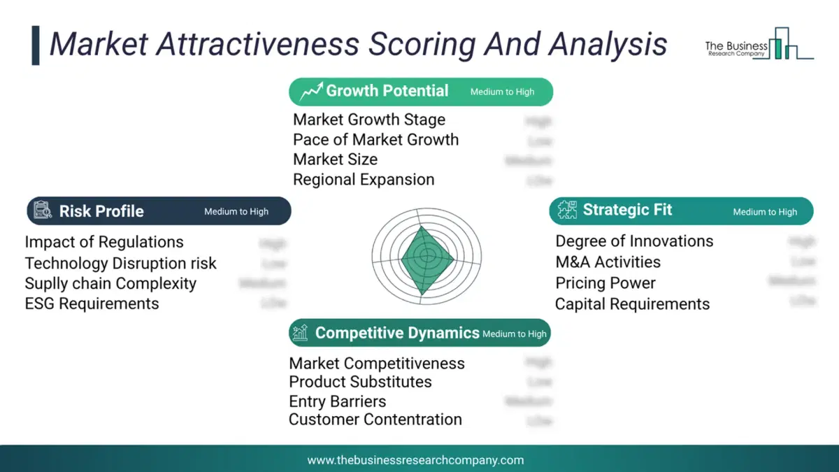
This chart presents market attractiveness based on a quantitative evaluation of growth, competition, strategic alignment, and risk, offering a clear view of opportunity areas for decision-making. This chart is for illustrative purposes; the full report contains the complete analysis.
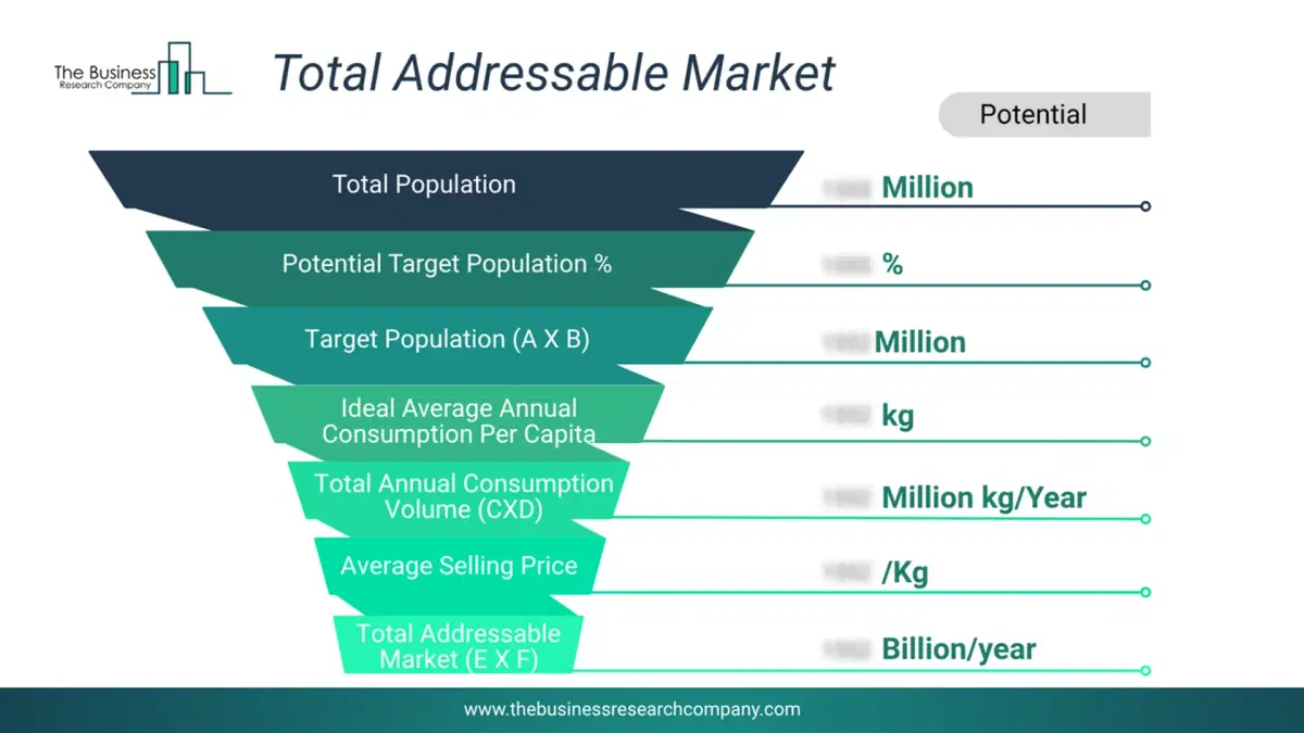
This chart highlights the Total Addressable Market (TAM) by estimating the maximum revenue opportunity using an assumption-driven approach, supporting strategic planning and opportunity sizing across markets. The chart is illustrative; the full report provides a more comprehensive analysis.
What Key Data and Analysis Are Included in the Semiconductor And Integrated Circuit (IC) Packaging Materials Market Report 2026?
The semiconductor and integrated circuit (ic) packaging materials market research report is one of a series of new reports from The Business Research Company that provides semiconductor and integrated circuit (ic) packaging materials market statistics, including semiconductor and integrated circuit (ic) packaging materials industry global market size, regional shares, competitors with a semiconductor and integrated circuit (ic) packaging materials market share, detailed semiconductor and integrated circuit (ic) packaging materials market segments, market trends and opportunities, and any further data you may need to thrive in the semiconductor and integrated circuit (ic) packaging materials industry. This semiconductor and integrated circuit (ic) packaging materials market research report delivers a complete perspective of everything you need, with an in-depth analysis of the current and future scenario of the industry.Semiconductor And Integrated Circuit (IC) Packaging Materials Market Report Forecast Analysis
| Report Attribute | Details |
|---|---|
| Market Size Value In 2026 | $56.2 billion |
| Revenue Forecast In 2030 | $86.15 billion |
| Growth Rate | CAGR of 11.3% from 2026 to 2030 |
| Base Year For Estimation | 2025 |
| Actual Estimates/Historical Data | 2020-2025 |
| Forecast Period | 2026 - 2030 |
| Market Representation | Revenue in USD Billion and CAGR from 2026 to 2030 |
| Segments Covered | Type, Packaging Technology, Application, End Use Industry |
| Regional Scope | Asia-Pacific, Western Europe, Eastern Europe, North America, South America, Middle East, Africa |
| Country Scope | The countries covered in the report are Australia, Brazil, China, France, Germany, India, Indonesia, Japan, Taiwan, Russia, South Korea, UK, USA, Canada, Italy, Spain. |
| Key Companies Profiled | Ajinomoto Co. Inc., Amkor Technology, AT&S Austria Technologie & Systemtechnik Aktiengesellschaft, California Fine Wire Co., Chang Wah Technology Co. Ltd., Haesung DS Co. Ltd., Heraeus Electronics GmbH & Co. KG, Ibiden Co. Ltd., Kinsus Interconnect Technology Corp., Kyocera Corporation, Merck KGaA, Mitsui Chemicals Inc., MK Electron Co. Ltd., Namics Corporation, Nan Ya Printed Circuit Board Corporation, Niterra Co. Ltd., Resonac Holdings Corporation, Senju Metal Industry Co. Ltd., Shin-Etsu Chemical Co. Ltd., Shinko Electric Industries Co. Ltd., Sumitomo Bakelite Co. Ltd., TANAKA Precious Metal Technologies Co. Ltd., Unimicron Technology Corporation. |
| Customization Scope | Request for Customization |
| Pricing And Purchase Options | Explore Purchase Options |