

Semiconductor Metrology And Inspection Market Report 2026
Global Outlook – By Type ( Optical, E-Beam), By Lithography Metrology ( Overlay, Dimension Equipment, Mask Inspection And Metrology), By Application ( Lithography Metrology, Wafer Inspection, Thin Film Metrology) – Market Size, Trends, Strategies, and Forecast to 2030
Semiconductor Metrology And Inspection Market Overview
• Semiconductor Metrology And Inspection market size has reached to $8.34 billion in 2025 • Expected to grow to $11.47 billion in 2030 at a compound annual growth rate (CAGR) of 6.6% • Growth Driver: Rise In Consumer Electronics To Drive Market Growth • Market Trend: Product Innovations Transforming The Semiconductor Metrology And Inspection Market • Asia-Pacific was the largest region and fastest growing region.Market Gains By 2030 – Top Opportunities By Segment
Market Gain identifies the most promising market opportunities by highlighting the segments or products expected to generate the highest incremental revenue growth over the next five years.
What Is Covered Under Semiconductor Metrology And Inspection Market?
Semiconductor metrology and inspection are crucial tools for making sure that every step of the semiconductor production process is completed to the highest level feasible. Inspection detects surface particles, pattern errors, and other factors that may affect the performance of the finished device, while metrological methods confirm that the desired physical and electrical parameters of the devices under production are satisfied at every step. The main types of semiconductor metrology and inspection are optical and e-beam. Optical inspection of semiconductors refers inspection where measurements are taken using light and its reflections. The two main categories of optical inspection are brightfield and darkfield. Darkfield inspection instruments measure a reduced angle of light reflection. The factory's mainstay technology, brightfield inspection, measures light coming from a higher angle. The lithography metrology consists of overlay, dimension equipment, and mask inspection and metrology. The main types of semiconductor metrology and inspection is used in lithography metrology, wafer inspection, and thin film metrology.
What Is The Semiconductor Metrology And Inspection Market Size 2026 And Growth Rate?
The semiconductor metrology and inspection market size has grown strongly in recent years. It will grow from $8.34 billion in 2025 to $8.88 billion in 2026 at a compound annual growth rate (CAGR) of 6.5%. The growth in the historic period can be attributed to increasing need for precision inspection in lithography, rising complexity of semiconductor device geometries, growing demand for wafer defect detection, expansion of thin-film metrology applications, evolution of e-beam inspection platforms.What Is The Semiconductor Metrology And Inspection Market Growth Forecast?
The semiconductor metrology and inspection market size is expected to see strong growth in the next few years. It will grow to $11.47 billion in 2030 at a compound annual growth rate (CAGR) of 6.6%. The growth in the forecast period can be attributed to rising production of advanced nodes below 5nm, growing need for automated high-throughput metrology, expansion of 3d packaging inspection requirements, increased reliance on ai-based inspection analytics, rising investment in semiconductor fabs worldwide. Major trends in the forecast period include advancement of AI-driven defect detection, adoption of intelligent semiconductor manufacturing, growth of cloud-enabled inspection systems, expansion of connected metrology platforms, development of autonomous wafer inspection solutions.

Global Semiconductor Metrology And Inspection Market Segmentation
1) By Type: Optical, E-Beam 2) By Lithography Metrology: Overlay, Dimension Equipment, Mask Inspection And Metrology 3) By Application: Lithography Metrology, Wafer Inspection, Thin Film Metrology Subsegments: 1) By Optical: Optical Inspection Systems, Scatterometry, Interferometry, Reflective Measurement Systems 2) By E-Beam: E-Beam Inspection Systems, E-Beam Metrology Systems, E-Beam Lithography Tools The top segments in the semiconductor metrology and inspection market will be: • Optical will reach $6287.7 Million by 2030. • Wafer Inspection will reach $5168.49 Million by 2030. • Lithography Metrology will reach $4349.98 Million by 2030. • E-Beam will reach $3789.18 Million by 2030. • Thin Film Metrology will reach $2171.07 Million by 2030.What Is The Driver Of The Semiconductor Metrology And Inspection Market?
The increase in consumer electronics is expected to propel the growth of the semiconductor metrology and inspection market going forward. Increased demand for semiconductors in devices like smartphones and IoT gadgets necessitates precise manufacturing processes. Stringent quality standards for consumer electronics drive the use of advanced metrology tools to detect defects. Miniaturization trends in electronics require accurate measurement processes, and technological innovation in consumer electronics relies on continuous advancements in semiconductor manufacturing technologies. For instance, in May 2023, according to the Japan Electronics and Information Technology Industries Association, a Japan-based trade association, the total electronic equipment production in Japan reached 771,457 units. In addition, consumer electronics production reached 32,099 units in May 2023, compared to 25,268 units in May 2022. Therefore, the increase in consumer electronics is driving the growth of the semiconductor metrology and inspection industry.
Infographic Chart Showing Key Market Drivers Analysis And Restraints For Semiconductor Metrology And Inspection Market
The chart presents an impact analysis of key drivers and restraints, quantifying their relative influence on the market's growth rate and helping assess the balance between growth enablers and limiting factors. This chart offers a high-level perspective; the full report contains more detailed insights.
How Will The Drivers Impact Growth In The Global Semiconductor Metrology And Inspection Market?
• Government Investments In Domestic Semiconductor Manufacturing (Medium) – During the forecast period, the government investments in domestic semiconductor manufacturing are expected to propel the growth of the semiconductor metrology and inspection market in the forecast period. increasing public funding and policy support for local semiconductor production are encouraging the establishment of new fabrication facilities and the expansion of existing manufacturing capabilities. these initiatives require advanced metrology and inspection solutions to ensure precise measurement, defect detection, and process control across increasingly complex semiconductor fabrication processes. semiconductor metrology and inspection systems provide essential capabilities for maintaining quality standards, improving yield, and supporting high-volume manufacturing in advanced nodes. as governments worldwide prioritize semiconductor self-sufficiency and supply chain resilience, manufacturers are increasingly investing in advanced metrology and inspection technologies to support new fabs and technology development, thereby boosting market adoption. therefore, government investments in domestic semiconductor manufacturing will drive the growth of the semiconductor metrology and inspection market. the government investments in domestic semiconductor manufacturing growth contribution during the forecast period in 2025 is 1.5%. • Expansion Of 5G Communication Infrastructure (Medium) – During the forecast period, the expansion of 5G communication infrastructure is expected to propel the growth of the semiconductor metrology and inspection market. The rapid deployment of 5G networks requires advanced semiconductor components with higher performance, smaller node sizes, and complex architectures. These requirements encourage semiconductor manufacturers to adopt precise metrology and inspection systems to ensure device accuracy, detect defects, and maintain high production yields. Semiconductor metrology and inspection solutions provide reliable measurement and quality control capabilities that support the fabrication of advanced chips used in 5G base stations, network equipment, and connected devices. As investments in 5G infrastructure continue to increase across telecommunications and electronics industries, companies are increasingly implementing advanced inspection technologies to improve process control and product reliability, thereby boosting market adoption. Therefore, the expansion of 5G communication infrastructure will drive the growth of the semiconductor metrology and inspection market. The expansion of 5G communication infrastructure growth contribution during the forecast period in 2025 is 1.3%. • Rapid Growth Of IoT Devices And Connected Technologies (Medium) – During the forecast period, the rapid growth of iot devices and connected technologies is expected to propel the growth of the semiconductor metrology and inspection market in the forecast period. the increasing adoption of smart devices, connected sensors, industrial iot systems, and smart home technologies is significantly raising the demand for advanced semiconductor chips. these chips require high precision and defect-free manufacturing to ensure reliable connectivity and performance. as a result, semiconductor manufacturers are increasingly deploying advanced metrology and inspection systems to monitor process accuracy and maintain high yield. additionally, the miniaturization and complexity of iot semiconductor components further increase the need for precise measurement and defect detection solutions. this growing iot ecosystem is therefore strengthening the demand for advanced semiconductor metrology and inspection technologies. the rapid growth of iot devices and connected technologies growth contribution during the forecast period in 2025 is 1.0%. • Growth In Automotive Electronics And Electric Vehicles (Low) – During the forecast period, growth in automotive electronics and electric vehicles is expected to propel the growth of the semiconductor metrology and inspection market. The increasing integration of advanced semiconductor components in electric vehicles and modern automotive electronics requires highly precise manufacturing and quality control processes. Semiconductor metrology and inspection solutions help manufacturers ensure accurate measurement, detection, and process control across complex semiconductor devices used in power electronics, sensors, and advanced driver-assistance systems. As automotive manufacturers continue to adopt electrification and intelligent electronic systems, the demand for reliable semiconductor production and testing technologies is rising. Therefore, growth in automotive electronics and electric vehicles will drive the growth of the semiconductor metrology and inspection market. The growth in automotive electronics and electric vehicles growth contribution during the forecast period in 2025 is 0.8%.How Will The Restraints Impact Growth In The Global Semiconductor Metrology And Inspection Market?
• Complex Integration Of Advanced Inspection Technologies In Semiconductor Fabrication Facilities (Medium) – During the forecast period, complex integration of advanced inspection technologies in semiconductor fabrication facilities is expected to hinder the growth of the semiconductor metrology and inspection market in the forecast period. semiconductor manufacturing environments involve highly complex and tightly controlled production processes that rely on multiple interconnected systems such as lithography, deposition, etching, and process control platforms. the deployment of advanced metrology and inspection tools requires seamless integration with these existing manufacturing systems to ensure accurate measurement, real-time monitoring, and effective process optimization. achieving such integration often requires significant engineering effort, software customization, and compatibility adjustments across different hardware and data management platforms. for several semiconductor manufacturers, particularly those operating mature fabrication facilities, these technical complexities may outweigh the immediate operational advantages, leading to slower technology adoption. therefore, complex integration of advanced inspection technologies in semiconductor fabrication facilities may hinder the growth of the semiconductor metrology and inspection market. growth affected by the complex integration of advanced inspection technologies in semiconductor fabrication facilities during the forecast period in 2025 is -1.5%. • Shortage Of Skilled Semiconductor Engineers And Technical Experts (Medium) – During the forecast period, shortage of skilled semiconductor engineers and technical experts is expected to hinder the growth of the semiconductor metrology and inspection market in the forecast period. semiconductor metrology and inspection systems require highly specialized professionals with expertise in semiconductor physics, process control, advanced lithography, yield analysis, and data analytics. however, the rapid expansion of semiconductor fabrication facilities and advanced packaging technologies has significantly increased the demand for qualified engineers and technicians, creating a global talent gap. as a result, companies often face challenges in recruiting and retaining professionals capable of operating complex metrology tools, analyzing defect patterns, and managing high-precision inspection processes. for many organizations, particularly emerging semiconductor manufacturers and research facilities, limited access to skilled talent can slow the adoption of advanced metrology and inspection solutions despite growing technological requirements. therefore, the shortage of skilled semiconductor engineers and technical experts may hinder the growth of the semiconductor metrology and inspection market. growth affected by the shortage of skilled semiconductor engineers and technical experts during the forecast period in 2025 is -1.0%. • Impact Of Trade War And Tariff (Medium) – During the forecast period, trade wars and tariffs are expected to restrain the growth of the semiconductor metrology and inspection market during the forecast period by increasing the costs of imported precision components, optical systems, advanced sensors, high-performance computing modules, and specialized electronic subsystems used in metrology and inspection equipment. many manufacturers rely on globally sourced components such as high-resolution imaging sensors, precision optics, semiconductor-grade electronics, motion control systems, and advanced computing hardware. higher import duties and cross-border trade restrictions can increase procurement costs and disrupt the highly globalized semiconductor supply chain, leading to price volatility and longer equipment delivery timelines. these additional costs may be transferred to semiconductor manufacturers, increasing the capital expenditure required for metrology and inspection tools used in wafer fabrication and advanced packaging processes. consequently, semiconductor fabs and equipment buyers may delay or reduce investments in new inspection and measurement systems, particularly during periods of geopolitical uncertainty. therefore, trade wars and tariffs may restrain the growth of the semiconductor metrology and inspection market. growth affected by the impact of trade wars and tariffs during the forecast period in 2025 is -0.3%.Key Players In The Global Semiconductor Metrology And Inspection Market
Major companies operating in the semiconductor metrology and inspection market are KLA Corporation, Applied Materials Inc., Onto Innovation Inc. (Rudolph Technologies Corporation), Thermo Fisher Scientific Inc., Hitachi High-Tech Corporation, Nova Measuring Instruments Ltd., ASML Holding NV, Lasertec Corporation, JEOL Ltd., Nikon Metrology NV, Camtek Limited, Bruker Corporation, Nanometrics Incorporated, Horiba Ltd., Carl Zeiss AG, SENTECH Instruments GmbH, Keyence Corporation, Accurion GmbH, Alicona Imaging GmbH, Veeco Instruments Inc., FormFactor Inc.
This chart is for illustrative purposes; the full report includes a detailed competitor analysis and comprehensive overview of the top 10 companies in the market.

This chart maps companies by product innovation and brand strength, with bubble size indicating relative revenue, helping identify market leaders, challengers, and niche players. This is an illustrative chart; the full report provides a complete and accurate competitive analysis.
Global Semiconductor Metrology And Inspection Market Trends and Insights
Major companies operating in the semiconductor metrology and inspection market are focusing on innovating new technologies to improve the inspection process and ensure the quality of semiconductor devices. In March 2024, Hitachi High‑Tech Corporation, a Japan‑based advanced technology equipment manufacturer, introduced the LS9300AD wafer inspection system, featuring a built-in Differential Interference Contrast (DIC) optical system for high-sensitivity detection of microscopic defects, a DIC-compatible data processing system that enables simultaneous dark-field laser scattering and DIC inspection mapping, and a true wafer-edge-grip method that allows front and back surface inspection of non-patterned wafers. This innovation strengthens Hitachi High‑Tech’s capabilities in the semiconductor metrology and inspection market.What Are Latest Mergers And Acquisitions In The Semiconductor Metrology And Inspection Market?
In September 2023, Camtek Ltd., an Israel-based provider of automated inspection and metrology equipment for semiconductor wafers and advanced packaging, acquired FRT Metrology GmbH for US$100 million in cash. With this acquisition, Camtek aimed to strengthen its semiconductor metrology and inspection product portfolio by integrating FRT’s high-precision solutions for advanced packaging and silicon carbide wafers, enhancing technological capabilities and market position. FRT Metrology GmbH is a Germany-based provider of high-precision metrology systems for advanced semiconductor packaging, silicon carbide wafers, and three-dimensional integrated circuit applications.
Regional Outlook
Asia-Pacific was the largest region in the semiconductor metrology and inspection market in 2025. Asia-Pacific is expected to be the fastest-growing region in the forecast period. The regions covered in this market report are Asia-Pacific, South East Asia, Western Europe, Eastern Europe, North America, South America, Middle East, Africa. The countries covered in this market report are Australia, Brazil, China, France, Germany, India, Indonesia, Japan, Taiwan, Russia, South Korea, UK, USA, Canada, Italy, Spain.What Defines the Semiconductor Metrology And Inspection Market?
The semiconductor metrology and inspection market includes revenues earned by lithography metrology and wafer inspection. The market value includes the value of related goods sold by the service provider or included within the service offering. Only goods and services traded between entities or sold to end consumers are included.How is Market Value Defined and Measured?
The market value is defined as the revenues that enterprises gain from the sale of goods and/or services within the specified market and geography through sales, grants, or donations in terms of the currency (in USD unless otherwise specified). The revenues for a specified geography are consumption values that are revenues generated by organizations in the specified geography within the market, irrespective of where they are produced. It does not include revenues from resales along the supply chain, either further along the supply chain or as part of other products.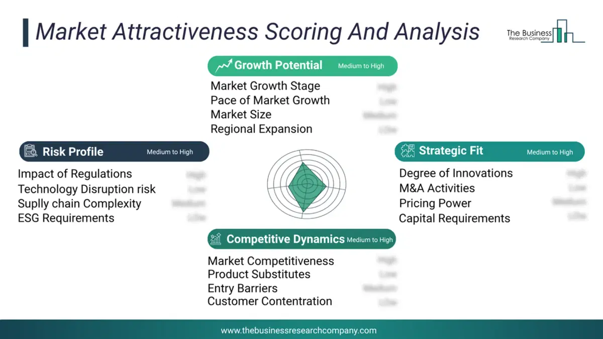
This chart presents market attractiveness based on a quantitative evaluation of growth, competition, strategic alignment, and risk, offering a clear view of opportunity areas for decision-making. This chart is for illustrative purposes; the full report contains the complete analysis.
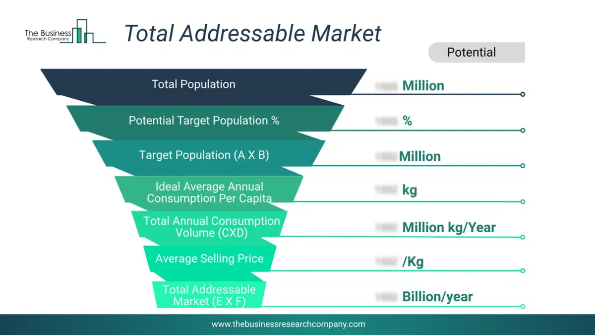
This chart highlights the Total Addressable Market (TAM) by estimating the maximum revenue opportunity using an assumption-driven approach, supporting strategic planning and opportunity sizing across markets. The chart is illustrative; the full report provides a more comprehensive analysis.
What Key Data and Analysis Are Included in the Semiconductor Metrology And Inspection Market Report 2026?
The semiconductor metrology and inspection market research report is one of a series of new reports from The Business Research Company that provides market statistics, including industry global market size, regional shares, competitors with the market share, detailed market segments, market trends and opportunities, and any further data you may need to thrive in the semiconductor metrology and inspection industry. The market research report delivers a complete perspective of everything you need, with an in-depth analysis of the current and future state of the industry.Semiconductor Metrology And Inspection Market Report 2026 Market Report Forecast Analysis
| Report Attribute | Details |
|---|---|
| Market Size Value In 2026 | $8.88 billion |
| Revenue Forecast In 2030 | $11.47 billion |
| Growth Rate | CAGR of 6.5% from 2026 to 2030 |
| Base Year For Estimation | 2025 |
| Actual Estimates/Historical Data | 2020-2025 |
| Forecast Period | 2026 - 2030 - 2035 |
| Market Representation | Revenue in USD Billion and CAGR from 2026 to 2030 |
| Segments Covered | Type, Lithography Metrology, Application |
| Regional Scope | Asia-Pacific, Western Europe, Eastern Europe, North America, South America, Middle East, Africa |
| Country Scope | The countries covered in the report are Australia, Brazil, China, France, Germany, India, Indonesia, Japan, Taiwan, Russia, South Korea, UK, USA, Canada, Italy, Spain. |
| Key Companies Profiled | KLA Corporation, Applied Materials Inc., Onto Innovation Inc. (Rudolph Technologies Corporation), Thermo Fisher Scientific Inc., Hitachi High-Tech Corporation, Nova Measuring Instruments Ltd., ASML Holding NV, Lasertec Corporation, JEOL Ltd., Nikon Metrology NV, Camtek Limited, Bruker Corporation, Nanometrics Incorporated, Horiba Ltd., Carl Zeiss AG, SENTECH Instruments GmbH, Keyence Corporation, Accurion GmbH, Alicona Imaging GmbH, Veeco Instruments Inc., FormFactor Inc. |
| Customization Scope | Request for Customization |
| Pricing And Purchase Options | Explore Purchase Options |