

2 Nanometer (nm) And Beyond Semiconductor Node Market Report 2026
Global Outlook – By Process Node (2 Nanometer, 1.8 Nanometer, 1.4 Nanometer, Below 1.4 Nanometer), By Transistor Architecture (Complementary Field-Effect Transistors, Nanosheet Transistors, Forksheet Transistors), By End Use Industry (Consumer Electronics, Data Centers And Cloud Computing, Automotive Industry, Aerospace And Defense, High-Performance Computing) – Market Size, Trends, Strategies, and Forecast to 2030
2 Nanometer (nm) And Beyond Semiconductor Node Market Overview
• 2 Nanometer (nm) And Beyond Semiconductor Node market size has reached to $23.46 billion in 2025 • Expected to grow to $53.35 billion in 2030 at a compound annual growth rate (CAGR) of 17.8% • Growth Driver: Increasing Demand For High-Performance Computing (HPC) Driving The Market Growth Due To Growing Need For Advanced Semiconductor Processing Capabilities • Market Trend: Technological Advancements In Atomic Layer Deposition Systems For Next-Generation Semiconductor Nodes And Advanced Chip Manufacturing • North America was the largest region in 2025 and Asia-Pacific is the fastest growing region.What Is Covered Under 2 Nanometer (nm) And Beyond Semiconductor Node Market?
2 nanometer (nm) and beyond semiconductor nodes refer to advanced semiconductor manufacturing processes used to produce integrated circuits with extremely small feature dimensions and high transistor density. These nodes enable improvements in processing performance, power efficiency, chip integration, and computing capabilities while supporting the development of advanced electronic devices and systems. The manufacturing of these nodes relies on advanced lithography, semiconductor materials, process control, fabrication techniques, and precision manufacturing technologies. The main process nodes in the 2 nanometer (nm) and beyond semiconductor node include 2 nanometer, 1.8 nanometer, 1.4 nanometer, and below 1.4 nanometer. 2 nanometer refers to an advanced semiconductor manufacturing process designed to deliver higher transistor density, improved performance, and greater energy efficiency. These technologies use complementary field-effect transistors, nanosheet transistors, and forksheet transistors. They find application industries including consumer electronics, data centers and cloud computing, automotive industry, aerospace and defense, and high-performance computing.
What Is The 2 Nanometer (nm) And Beyond Semiconductor Node Market Size and Share 2026?
The 2 nanometer (nm) and beyond semiconductor node market size has grown rapidly in recent years. It will grow from $23.46 billion in 2025 to $27.72 billion in 2026 at a compound annual growth rate (CAGR) of 18.2%. The growth in the historic period can be attributed to increasing demand for high-performance computing, rising semiconductor transistor density requirements, growing adoption of advanced lithography, increasing demand for power-efficient integrated circuits, expanding semiconductor fabrication capacity.What Is The 2 Nanometer (nm) And Beyond Semiconductor Node Market Growth Forecast?
The 2 nanometer (nm) and beyond semiconductor node market size is expected to see rapid growth in the next few years. It will grow to $53.35 billion in 2030 at a compound annual growth rate (CAGR) of 17.8%. The growth in the forecast period can be attributed to rising demand for AI accelerator chips, growing data center computing requirements, increasing adoption of advanced automotive electronics, rising demand for energy-efficient semiconductor devices, expanding production of sub-2-nanometer chips. Major trends in the forecast period include increasing adoption of gate-all-around transistor architectures, growing use of backside power delivery networks, rising deployment of high-na extreme ultraviolet lithography, increasing development of nanosheet and forksheet transistor structures, growing demand for advanced semiconductor process control and precision manufacturing.Tariff Impact On 2 Nanometer (nm) And Beyond Semiconductor Node Market
Tariffs are impacting the 2 nanometer (nm) and beyond semiconductor nodes market by increasing the cost of imported semiconductor manufacturing equipment, advanced materials, lithography systems, and precision components required for leading-edge semiconductor fabrication. This is increasing production costs and potentially slowing advanced-node fab expansions, particularly in regions dependent on imported semiconductor equipment and materials such as Asia-Pacific and Europe. Hardware-intensive areas such as advanced lithography equipment, semiconductor fabrication systems, and process materials are most affected due to global supply chain dependencies. However, tariffs are also encouraging domestic semiconductor manufacturing, regional supplier diversification, localized equipment production, and increased investment in advanced fabrication infrastructure, creating greater long-term supply-chain resilience.

Global 2 Nanometer nm And Beyond Semiconductor Node Market Segmentation
1) By Process Node: 2 Nanometer, 1.8 Nanometer, 1.4 Nanometer, Below 1.4 Nanometer 2) By Transistor Architecture: Complementary Field-Effect Transistors, Nanosheet Transistors, Forksheet Transistors 3) By End Use Industry: Consumer Electronics, Data Centers And Cloud Computing, Automotive Industry, Aerospace And Defense, High-Performance Computing Subsegments: 1) By 2 Nanometer: Gate-All-Around 2 Nanometer Process, Nanosheet 2 Nanometer Process, RibbonFET 2 Nanometer Process, Backside Power Delivery 2 Nanometer Process, High-NA Extreme Ultraviolet 2 Nanometer Process 2) By 1.8 Nanometer: Gate-All-Around 1.8 Nanometer Process, Nanosheet 1.8 Nanometer Process, RibbonFET 1.8 Nanometer Process, Backside Power Delivery 1.8 Nanometer Process, High-NA Extreme Ultraviolet 1.8 Nanometer Process 3) By 1.4 Nanometer: Gate-All-Around 1.4 Nanometer Process, Nanosheet 1.4 Nanometer Process, RibbonFET 1.4 Nanometer Process, Backside Power Delivery 1.4 Nanometer Process, High-NA Extreme Ultraviolet 1.4 Nanometer Process 4) By Below 1.4 Nanometer: Gate-All-Around Below 1.4 Nanometer Process, Nanosheet Below 1.4 Nanometer Process, Forksheet Transistor Below 1.4 Nanometer Process, Complementary Field-Effect Transistor Below 1.4 Nanometer Process, Backside Power Delivery Below 1.4 Nanometer ProcessWhat Is The Driver Of The 2 Nanometer (nm) And Beyond Semiconductor Node Market?
The increasing demand for high-performance computing (HPC) is expected to propel the growth of the 2 nanometer (nm) and beyond semiconductor node market going forward. High-performance computing (HPC) refers to the use of advanced computing systems and processors to perform complex calculations and process large volumes of data at significantly higher speeds than conventional computing systems. The demand for high-performance computing is rising due to the rapid growth of artificial intelligence (AI), as AI applications require significant computational power, faster data processing, and advanced hardware capabilities to handle complex workloads and large volumes of data. Rising demand for high-performance computing drives the demand for 2 nanometer (nm) and beyond semiconductor nodes by increasing the need for advanced semiconductor technologies that deliver higher transistor density, improved processing performance, lower power consumption, and greater computational efficiency. For instance, in June 2025, according to TOP500, a Germany-based ranking system that maintains the global ranking of supercomputers, the combined performance of the world's 500 most powerful supercomputers increased from 11.72 exaflops in November 2024 to 13.84 exaflops in June 2025, representing an 18.1% increase. Therefore, the increasing demand for high-performance computing (HPC) is driving the growth of the 2 nanometer (nm) and beyond semiconductor node industry.Key Players In The Global 2 Nanometer (nm) And Beyond Semiconductor Node Market
Major companies operating in the 2 nanometer (nm) and beyond semiconductor node market are Advantest Corporation, Air Liquide S.A., Applied Materials Inc., ASML Holding N.V., Cadence Design Systems Inc., Canon Inc., Carl Zeiss AG, HORIBA Ltd., IBM Corporation, Intel Corporation, KLA Corporation, Lam Research Corporation, Lasertec Corporation, Merck KGaA, Onto Innovation Inc., Rapidus Corporation, Resonac Holdings Corporation, Samsung Electronics Co. Ltd., SCREEN Holdings Co. Ltd., Shin-Etsu Chemical Co. Ltd., Siltronic AG, Soitec S.A., SUMCO Corporation, Synopsys Inc., Taiwan Semiconductor Manufacturing Company Limited, Teradyne Inc., Tokyo Electron Limited, Tokyo Ohka Kogyo Co. Ltd., Ultra Clean Holdings Inc., Veeco Instruments Inc.
This chart is for illustrative purposes; the full report includes a detailed competitor analysis and comprehensive overview of the top 10 companies in the market.

This chart maps companies by product innovation and brand strength, with bubble size indicating relative revenue, helping identify market leaders, challengers, and niche players. This is an illustrative chart; the full report provides a complete and accurate competitive analysis.
Global 2 Nanometer (nm) And Beyond Semiconductor Node Market Trends and Insights
Major companies operating in the 2 nanometer (nm) and beyond semiconductor node market are focusing on developing innovative solutions such as, atomic layer deposition (ALD) systems, to enhance transistor performance, energy efficiency, and advanced chip scaling. Atomic layer deposition systems are semiconductor manufacturing technologies that deposit ultra-thin, highly uniform material layers with atomic-level precision, enabling chipmakers to create smaller and more precisely controlled transistor contacts and interconnects compared with conventional deposition techniques. For instance, in February 2026, Applied Materials, Inc., a US-based semiconductor equipment company, launched the Centris Spectral Molybdenum ALD system, an innovative deposition technology designed for 2nm and beyond semiconductor nodes. The system selectively deposits monocrystalline molybdenum to replace traditional tungsten contacts in advanced transistors, helping reduce electrical resistance at the critical connection between transistors and copper wiring. Its quad-reactor architecture provides precision chemical delivery along with plasma and thermal processing capabilities for advanced film formation. The technology can reduce critical contact resistance by up to 15% compared with the company’s existing selective tungsten system, supporting faster transistor operation and improved energy efficiency. The Spectral system is being adopted by leading logic chipmakers for 2nm and below process nodes, supporting the development of next-generation AI chips.What Are Latest Mergers And Acquisitions In The 2 Nanometer (nm) And Beyond Semiconductor Node Market?
In June 2026, Cadence Design Systems Inc., a US-based electronic design automation (EDA) company that specializes in semiconductor design software, intellectual property (IP), and system design solutions, partnered with Samsung Electronics Co. Ltd. to expand Memory and Interface IP and certified design and analysis flows for Samsung Foundry’s second-generation 2nm process technology. Through this multi-year collaboration, Cadence Design Systems, Inc. and Samsung Electronics Co., Ltd. aim to accelerate the development of next-generation AI infrastructure and physical AI designs, enable advanced semiconductor and 3D-IC designs with improved performance, power efficiency, and time to market, expand support for high-speed interfaces including NVIDIA NVLink-C2C, PCIe, UCIe, SerDes, and leading memory interfaces, and provide certified agentic AI-optimized digital, custom, 3D-IC, and system design and analysis solutions for advanced-node semiconductor development. Samsung Electronics Co. Ltd. is a South Korea-based electronics company that specializes in providing 2 nm-class semiconductor manufacturing.
Regional Outlook
North America was the largest region in the 2 nanometer (nm) and beyond semiconductor node market in 2025. Asia-Pacific is expected to be the fastest-growing region in the forecast period. The regions covered in this market report are Asia-Pacific, South East Asia, Western Europe, Eastern Europe, North America, South America, Middle East, Africa. The countries covered in this market report are Australia, Brazil, China, France, Germany, India, Indonesia, Japan, Taiwan, Russia, South Korea, UK, USA, Canada, Italy, Spain.What Defines the 2 Nanometer (nm) And Beyond Semiconductor Node Market?
The 2 nanometer (nm) and beyond semiconductor node market consists of sales of semiconductor wafers, lithography equipment, deposition and etching equipment, process control equipment, semiconductor manufacturing materials, and fabrication equipment. Values in this market are ‘factory gate’ values, that is, the value of goods sold by the manufacturers or creators of the goods, whether to other entities (including downstream manufacturers, wholesalers, distributors, and retailers) or directly to end customers. The value of goods in this market includes related services sold by the creators of the goods.How is Market Value Defined and Measured?
The market value is defined as the revenues that enterprises gain from the sale of goods and/or services within the specified market and geography through sales, grants, or donations in terms of the currency (in USD unless otherwise specified). The revenues for a specified geography are consumption values that are revenues generated by organizations in the specified geography within the market, irrespective of where they are produced. It does not include revenues from resales along the supply chain, either further along the supply chain or as part of other products.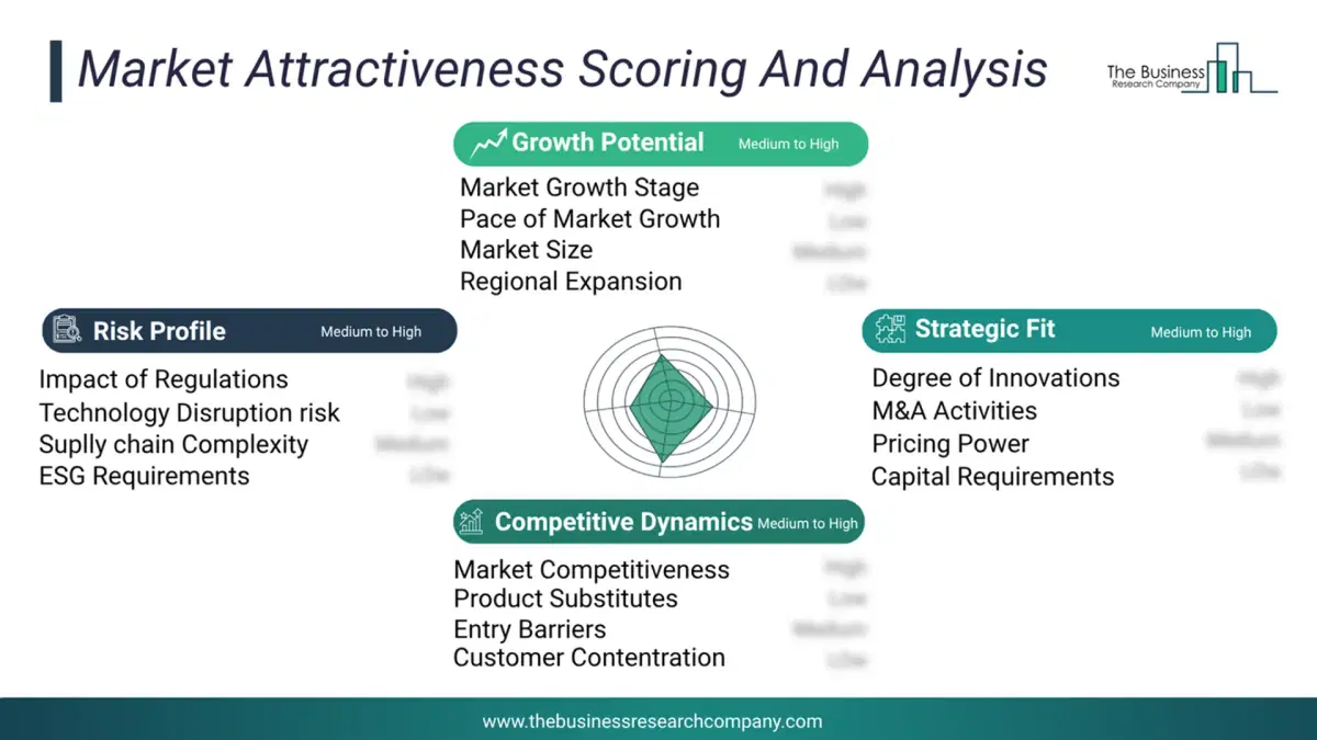
This chart presents market attractiveness based on a quantitative evaluation of growth, competition, strategic alignment, and risk, offering a clear view of opportunity areas for decision-making. This chart is for illustrative purposes; the full report contains the complete analysis.
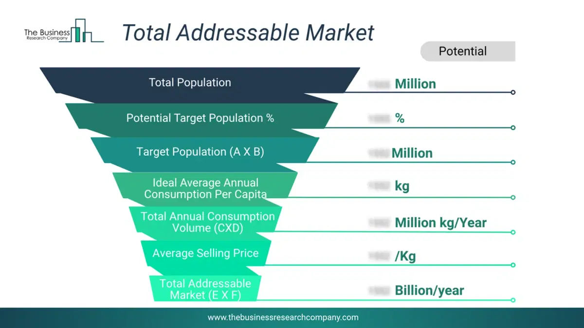
This chart highlights the Total Addressable Market (TAM) by estimating the maximum revenue opportunity using an assumption-driven approach, supporting strategic planning and opportunity sizing across markets. The chart is illustrative; the full report provides a more comprehensive analysis.
What Key Data and Analysis Are Included in the 2 Nanometer (nm) And Beyond Semiconductor Node Market Report 2026?
The 2 nanometer (nm) and beyond semiconductor node market research report is one of a series of new reports from The Business Research Company that provides market statistics, including industry global market size, regional shares, competitors with the market share, detailed market segments, market trends and opportunities, and any further data you may need to thrive in the 2 nanometer (nm) and beyond semiconductor node industry. The market research report delivers a complete perspective of everything you need, with an in-depth analysis of the current and future state of the industry.2 Nanometer (nm) And Beyond Semiconductor Node Market Report Forecast Analysis
| Report Attribute | Details |
|---|---|
| Market Size Value In 2026 | $27.72 billion |
| Revenue Forecast In 2030 | $53.35 billion |
| Growth Rate | CAGR of 17.8% from 2026 to 2030 |
| Base Year For Estimation | 2025 |
| Actual Estimates/Historical Data | 2020-2025 |
| Forecast Period | 2026 - 2030 |
| Market Representation | Revenue in USD Billion and CAGR from 2026 to 2030 |
| Segments Covered | Process Node, Transistor Architecture, End Use Industry |
| Regional Scope | Asia-Pacific, Western Europe, Eastern Europe, North America, South America, Middle East, Africa |
| Country Scope | The countries covered in the report are Australia, Brazil, China, France, Germany, India, Indonesia, Japan, Taiwan, Russia, South Korea, UK, USA, Canada, Italy, Spain. |
| Key Companies Profiled | Advantest Corporation, Air Liquide S.A., Applied Materials Inc., ASML Holding N.V., Cadence Design Systems Inc., Canon Inc., Carl Zeiss AG, HORIBA Ltd., IBM Corporation, Intel Corporation, KLA Corporation, Lam Research Corporation, Lasertec Corporation, Merck KGaA, Onto Innovation Inc., Rapidus Corporation, Resonac Holdings Corporation, Samsung Electronics Co. Ltd., SCREEN Holdings Co. Ltd., Shin-Etsu Chemical Co. Ltd., Siltronic AG, Soitec S.A., SUMCO Corporation, Synopsys Inc., Taiwan Semiconductor Manufacturing Company Limited, Teradyne Inc., Tokyo Electron Limited, Tokyo Ohka Kogyo Co. Ltd., Ultra Clean Holdings Inc., Veeco Instruments Inc. |
| Customization Scope | Request for Customization |
| Pricing And Purchase Options | Explore Purchase Options |