
Atomic Layer Etching Equipment Market Report 2026
Global Outlook – By Product (Thermal Atomic Layer Etching Equipment, Plasma Enhanced Atomic Layer Etching Equipment, Isotropic Atomic Layer Etching Equipment, Directional Atomic Layer Etching Equipment), By Wafer Size (200 Millimeter, 300 Millimeter, 450 Millimeter), By Application (Logic Devices, Memory Devices, Power Semiconductors, Microelectromechanical Systems, Advanced Packaging, Compound Semiconductors), By End User (Integrated Device Manufacturers, Foundries, Outsourced Semiconductor Assembly And Test Providers, Research Institutes And Universities) – Market Size, Trends, Strategies, and Forecast to 2030
Atomic Layer Etching Equipment Market Overview
• Atomic Layer Etching Equipment market size has reached to $1.23 billion in 2025 • Expected to grow to $1.91 billion in 2030 at a compound annual growth rate (CAGR) of 9.2% • Growth Driver: Rising Investment In Semiconductor Fabrication Facilities Fueling The Growth Of The Market Due To Increasing Demand For Atomic Scale Precision Manufacturing At Advanced Technology Nodes • Market Trend: Commercialization Of Atomic Layer Etching (ALE)-Based Patterning Platforms Enhances Precision In Advanced Semiconductor Manufacturing • North America was the largest region in 2025 and Asia-Pacific is the fastest growing region.What Is Covered Under Atomic Layer Etching Equipment Market?
Atomic layer etching (ALE) equipment is a semiconductor manufacturing tool that removes ultra-thin layers of material from a wafer with atomic-level precision using controlled, self-limiting chemical reactions. It enables highly accurate patterning and fabrication of advanced semiconductor devices. The main products of atomic layer etching equipment include thermal atomic layer etching equipment, plasma enhanced atomic layer etching equipment, isotropic atomic layer etching equipment, and directional atomic layer etching equipment. Thermal atomic layer etching equipment refers to etching systems that use controlled thermal chemical reactions to selectively remove material from semiconductor surfaces with atomic-scale precision. These equipment are available for wafer sizes of 200 millimeter, 300 millimeter, and 450 millimeter. The various applications involved are logic devices, memory devices, power semiconductors, microelectromechanical systems, advanced packaging, and compound semiconductors, and they are utilized by end users including integrated device manufacturers, foundries, outsourced semiconductor assembly and test providers, and research institutes and universities.
What Is The Atomic Layer Etching Equipment Market Size and Share 2026?
The atomic layer etching equipment market size has grown strongly in recent years. It will grow from $1.23 billion in 2025 to $1.34 billion in 2026 at a compound annual growth rate (CAGR) of 9.5%. The growth in the historic period can be attributed to increasing demand for advanced semiconductor devices, rising adoption of smaller semiconductor geometries, growing need for precise wafer material removal, increasing semiconductor manufacturing capacity, rising demand for advanced patterning processes.What Is The Atomic Layer Etching Equipment Market Growth Forecast?
The atomic layer etching equipment market size is expected to see strong growth in the next few years. It will grow to $1.91 billion in 2030 at a compound annual growth rate (CAGR) of 9.2%. The growth in the forecast period can be attributed to increasing demand for atomic-scale process control, rising adoption of advanced logic and memory devices, growing need for high-aspect-ratio etching, increasing demand for selective material removal, rising production of next-generation semiconductor architectures. Major trends in the forecast period include increasing adoption of atomic-level wafer processing, rising demand for high-precision semiconductor etching, growing use of self-limiting etching processes, increasing demand for advanced semiconductor device fabrication, rising focus on selective and damage-free material removal.
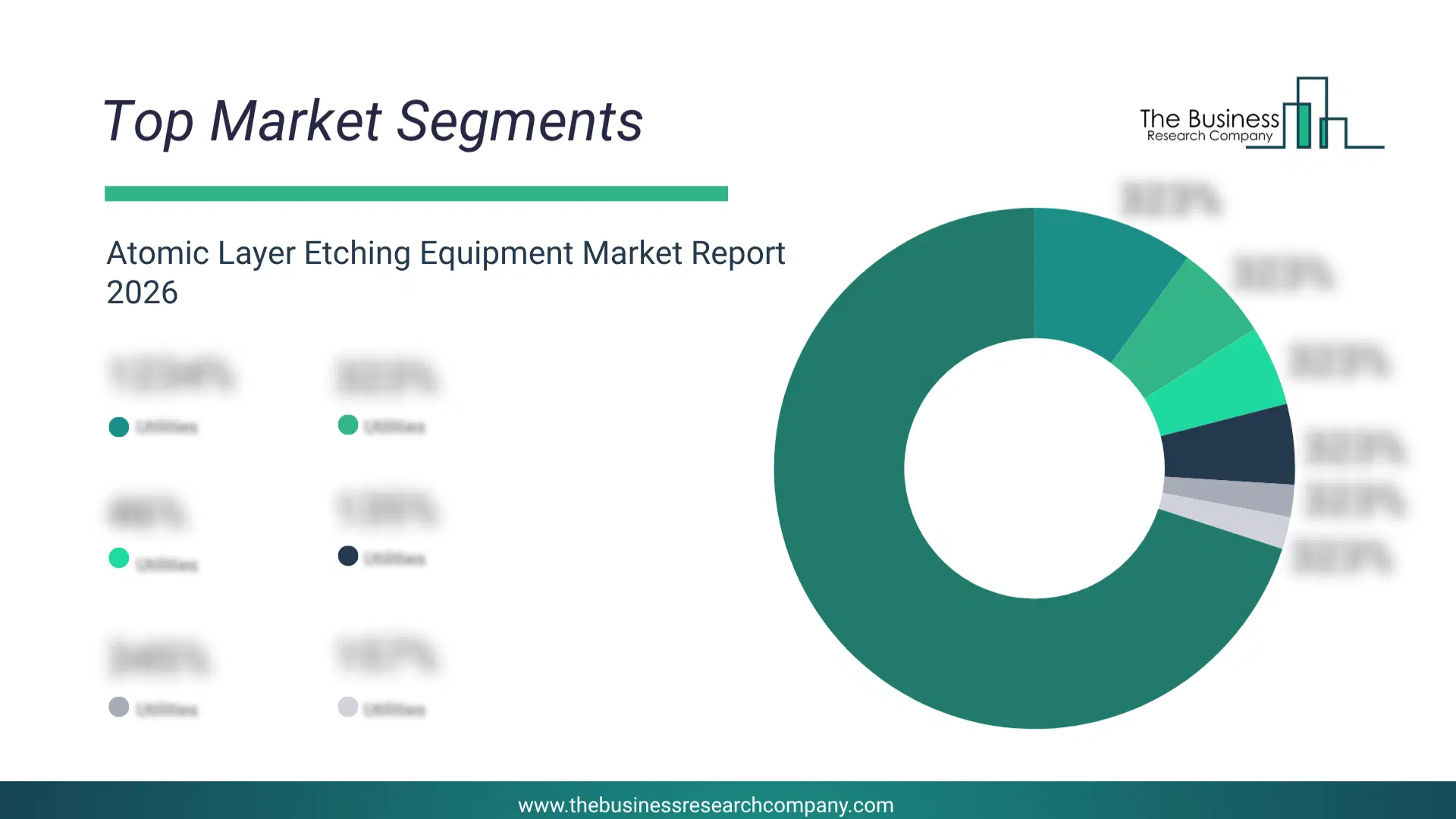
Global Atomic Layer Etching Equipment Market Segmentation
1) By Product: Thermal Atomic Layer Etching Equipment, Plasma Enhanced Atomic Layer Etching Equipment, Isotropic Atomic Layer Etching Equipment, Directional Atomic Layer Etching Equipment 2) By Wafer Size: 200 Millimeter, 300 Millimeter, 450 Millimeter 3) By Application: Logic Devices, Memory Devices, Power Semiconductors, Microelectromechanical Systems, Advanced Packaging, Compound Semiconductors 4) By End User: Integrated Device Manufacturers, Foundries, Outsourced Semiconductor Assembly And Test Providers, Research Institutes And Universities Subsegments: 1) By Thermal Atomic Layer Etching Equipment: Batch Thermal Atomic Layer Etching Equipment, Single Wafer Thermal Atomic Layer Etching Equipment 2) By Plasma Enhanced Atomic Layer Etching Equipment: Remote Plasma Atomic Layer Etching Equipment, Direct Plasma Atomic Layer Etching Equipment 3) By Isotropic Atomic Layer Etching Equipment: Chemical Isotropic Atomic Layer Etching Equipment, Plasma Assisted Isotropic Atomic Layer Etching Equipment 4) By Directional Atomic Layer Etching Equipment: Ion Beam Directional Atomic Layer Etching Equipment, Plasma Directional Atomic Layer Etching EquipmentWhat Is The Driver Of The Atomic Layer Etching Equipment Market?
The rising investment in semiconductor fabrication facilities is expected to propel the growth of the atomic layer etching equipment market going forward. Semiconductor fabrication facilities are specialized manufacturing plants where integrated circuits and semiconductor devices are produced through highly controlled processes such as deposition, lithography, etching, doping, and packaging. Investment in semiconductor fabrication facilities is rising due to the growing demand for advanced semiconductor chips used in artificial intelligence, high performance computing, 5G networks, electric vehicles, and consumer electronics, requiring expanded manufacturing capacity and more advanced production technologies. Higher investment in semiconductor fabrication facilities increases the adoption of atomic layer etching equipment as new and expanded fabrication plants require advanced etching technologies capable of achieving atomic scale precision, high selectivity, and precise process control for manufacturing increasingly complex semiconductor devices at advanced technology nodes. For instance, in August 2024, according to the Department of Commerce, a US-based government agency, more than $30 billion in proposed private-sector investments under the CHIPS and Science Act had been announced across 23 projects in 15 states, including 16 new semiconductor manufacturing facilities expected to create more than 115,000 manufacturing and construction jobs. Therefore, the rising investment in semiconductor fabrication facilities is driving the growth of the atomic layer etching equipment industry.Key Players In The Global Atomic Layer Etching Equipment Market
Major companies operating in the atomic layer etching equipment market are Applied Materials Inc, Tokyo Electron Limited, Lam Research Corporation, Hitachi Ltd, Canon Inc, ASM International N V, Kokusai Electric Corporation, NAURA Technology Group Co Ltd, ULVAC Inc, Advanced Micro-Fabrication Equipment Inc China, Veeco Instruments Inc, Oxford Instruments plc, Shibaura Mechatronics Corporation, Beneq Oy, Mattson Technology Inc, Jusung Engineering Co Ltd, Plasma-Therm LLC, Samco Inc, PVA TePla AG, SENTECH Instruments GmbH, Trion Technology Inc, AlixLabs AB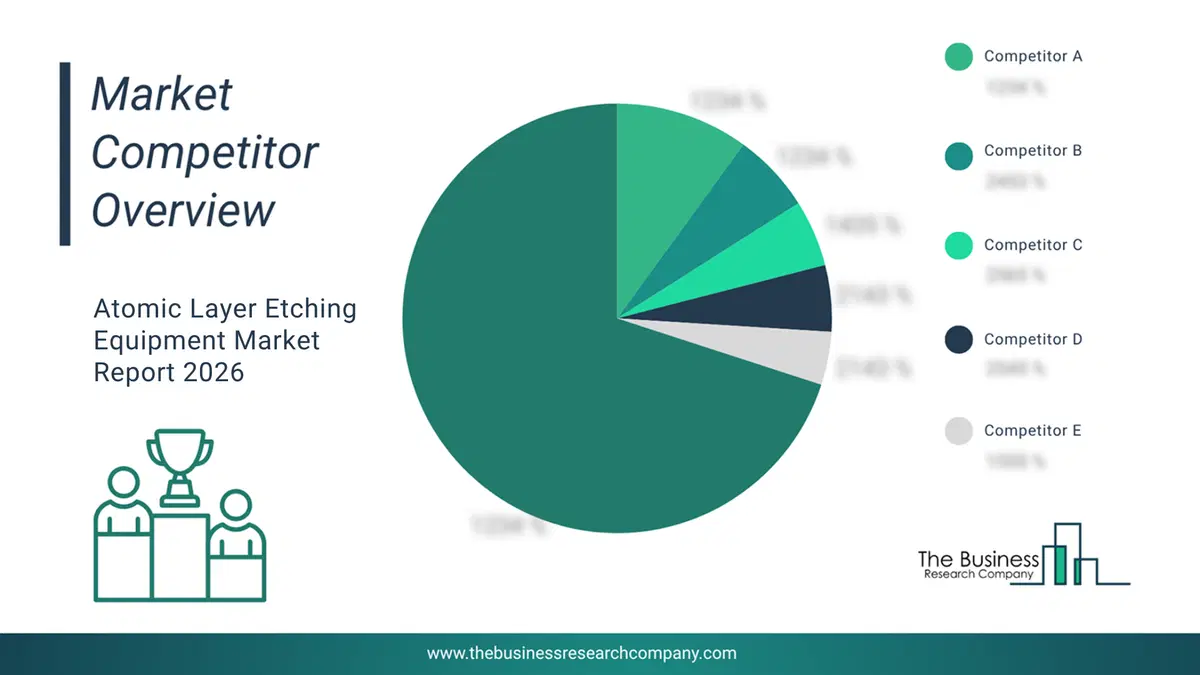
This chart is for illustrative purposes; the full report includes a detailed competitor analysis and comprehensive overview of the top 10 companies in the market.
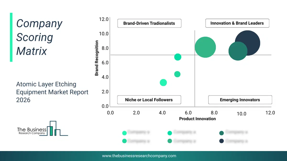
This chart maps companies by product innovation and brand strength, with bubble size indicating relative revenue, helping identify market leaders, challengers, and niche players. This is an illustrative chart; the full report provides a complete and accurate competitive analysis.
Global Atomic Layer Etching Equipment Market Trends and Insights
Major companies operating in the atomic layer etching equipment market are focusing on developing advanced solutions, such as atomic pitch splitting (APS)-based patterning platforms, to enable atomic-scale material removal, improve patterning precision, and support next-generation semiconductor manufacturing. Atomic pitch splitting (APS)-based patterning platforms are semiconductor processing systems that utilize atomic layer etching (ALE) to achieve atomic-scale pitch reduction with high selectivity, excellent uniformity, and minimal substrate damage while integrating with existing lithography workflows. For instance, in June 2026, AlixLabs AB, a Sweden-based semiconductor technology company, launched SAX FORMA, its next-generation semiconductor processing platform built for the angstrom era and powered by atomic pitch splitting (APS) technology based on atomic layer etching (ALE). Designed to enable atomic-scale patterning for advanced semiconductor manufacturing, the platform supports sub-10 nm feature fabrication with enhanced precision, improved process scalability, and reduced manufacturing complexity, addressing the requirements of next-generation logic and memory devices.What Are Latest Mergers And Acquisitions In The Atomic Layer Etching Equipment Market?
In April 2023, Oxford Instruments Plasma Technology, a UK-based provider of etch and deposition processing equipment, partnered with King Abdullah University of Science and Technology (KAUST), to upgrade its hardware and strengthen its advanced ALD research by integrating atomic layer etching (ALE) capability. As a result of the partnership, KAUST enhanced its semiconductor research infrastructure by adding two Oxford Instruments PlasmaPro100 Cobra Atomic Layer Etching (ALE) systems alongside its existing FlexAL Atomic Layer Deposition (ALD) platform. This strengthened KAUST's ability to advance world leading semiconductor research, particularly in GaN HEMT technologies, while accelerating the translation of academic innovations into industrial applications. King Abdullah University of Science and Technology (KAUST) is a Saudi Arabia-based science and technology research university.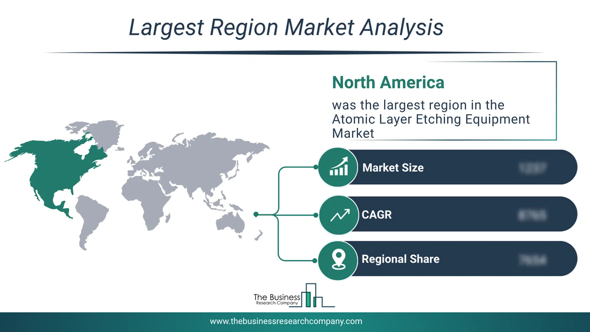
Regional Outlook
North America was the largest region in the atomic layer etching equipment market in 2025. Asia-Pacific is expected to be the fastest-growing region in the forecast period. The regions covered in this market report are Asia-Pacific, South East Asia, Western Europe, Eastern Europe, North America, South America, Middle East, Africa. The countries covered in this market report are Australia, Brazil, China, France, Germany, India, Indonesia, Japan, Taiwan, Russia, South Korea, UK, USA, Canada, Italy, Spain.What Defines the Atomic Layer Etching Equipment Market?
The atomic layer etching equipment market consists of sales of single wafer atomic layer etching systems, batch atomic layer etching systems, high aspect ratio etching systems, and silicon atomic layer etching equipment. Values in this market are ‘factory gate’ values, that is the value of goods sold by the manufacturers or creators of the goods, whether to other entities (including downstream manufacturers, wholesalers, distributors and retailers) or directly to end customers. The value of goods in this market includes related services sold by the creators of the goods.How is Market Value Defined and Measured?
The market value is defined as the revenues that enterprises gain from the sale of goods and/or services within the specified market and geography through sales, grants, or donations in terms of the currency (in USD unless otherwise specified). The revenues for a specified geography are consumption values that are revenues generated by organizations in the specified geography within the market, irrespective of where they are produced. It does not include revenues from resales along the supply chain, either further along the supply chain or as part of other products.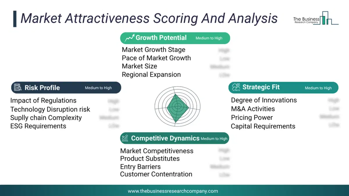
This chart presents market attractiveness based on a quantitative evaluation of growth, competition, strategic alignment, and risk, offering a clear view of opportunity areas for decision-making. This chart is for illustrative purposes; the full report contains the complete analysis.
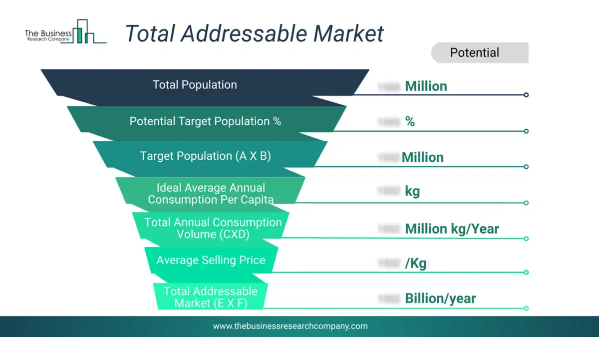
This chart highlights the Total Addressable Market (TAM) by estimating the maximum revenue opportunity using an assumption-driven approach, supporting strategic planning and opportunity sizing across markets. The chart is illustrative; the full report provides a more comprehensive analysis.
What Key Data and Analysis Are Included in the Atomic Layer Etching Equipment Market Report 2026?
The atomic layer etching equipment market research report is one of a series of new reports from The Business Research Company that provides market statistics, including industry global market size, regional shares, competitors with the market share, detailed market segments, market trends and opportunities, and any further data you may need to thrive in the atomic layer etching equipment industry. The market research report delivers a complete perspective of everything you need, with an in-depth analysis of the current and future state of the industry.Atomic Layer Etching Equipment Market Report Forecast Analysis
| Report Attribute | Details |
|---|---|
| Market Size Value In 2026 | $1.34 billion |
| Revenue Forecast In 2030 | $1.91 billion |
| Growth Rate | CAGR of 9.2% from 2026 to 2030 |
| Base Year For Estimation | 2025 |
| Actual Estimates/Historical Data | 2020-2025 |
| Forecast Period | 2026 - 2030 |
| Market Representation | Revenue in USD Billion and CAGR from 2026 to 2030 |
| Segments Covered | Product, Wafer Size, Application, End User |
| Regional Scope | Asia-Pacific, Western Europe, Eastern Europe, North America, South America, Middle East, Africa |
| Country Scope | The countries covered in the report are Australia, Brazil, China, France, Germany, India, Indonesia, Japan, Taiwan, Russia, South Korea, UK, USA, Canada, Italy, Spain. |
| Key Companies Profiled | Applied Materials Inc, Tokyo Electron Limited, Lam Research Corporation, Hitachi Ltd, Canon Inc, ASM International N V, Kokusai Electric Corporation, NAURA Technology Group Co Ltd, ULVAC Inc, Advanced Micro-Fabrication Equipment Inc China, Veeco Instruments Inc, Oxford Instruments plc, Shibaura Mechatronics Corporation, Beneq Oy, Mattson Technology Inc, Jusung Engineering Co Ltd, Plasma-Therm LLC, Samco Inc, PVA TePla AG, SENTECH Instruments GmbH, Trion Technology Inc, AlixLabs AB |
| Customization Scope | Request for Customization |
| Pricing And Purchase Options | Explore Purchase Options |