
Chip Photomask Market Report 2026
Global Outlook – By Type ( Binary Photomasks, Phase-Shifting Photomasks, Chromeless Photomasks, Other Types), By Application ( Semiconductor Manufacturing, Flat Panel Display Manufacturing, Micro-Electromechanical Systems (MEMS), Other Applications), By End-Use Industry ( Consumer Electronics, Automotive, Telecommunications, Healthcare) – Market Size, Trends, Strategies, and Forecast to 2030
Chip Photomask Market Overview
• Chip Photomask market size has reached to $4.81 billion in 2025 • Expected to grow to $5.63 billion in 2030 at a compound annual growth rate (CAGR) of 3.2% • Growth Driver: Growth In Consumer Electronics Driving Market Growth With Advancements In Smart Technology And Connectivity • Market Trend: Strategic Partnerships Driving Innovation In Chip Photomask Technology • Europe was the largest region in 2025 and Asia-Pacific is the fastest growing region.What Is Covered Under Chip Photomask Market?
A chip photomask is a high-precision, transparent plate containing a microscopic pattern used in semiconductor manufacturing to transfer circuit designs onto silicon wafers through photolithography. It acts as a stencil, enabling the production of integrated circuits (ICs) by selectively allowing light or other radiation to expose specific areas of a photoresist-coated wafer. The main types of chip photomasks are binary photomasks, phase-shifting photomasks, chromeless photomasks, and others. Binary photomasks are traditional masks with opaque and transparent regions, commonly used in semiconductor lithography for cost-effective pattern transfer to silicon wafers in digital device manufacturing. It is applicable in various applications such as semiconductor manufacturing, flat panel display manufacturing, micro-electromechanical systems (MEMS), and others and is used by several end-use industries, including consumer electronics, automotive, telecommunications, and healthcare.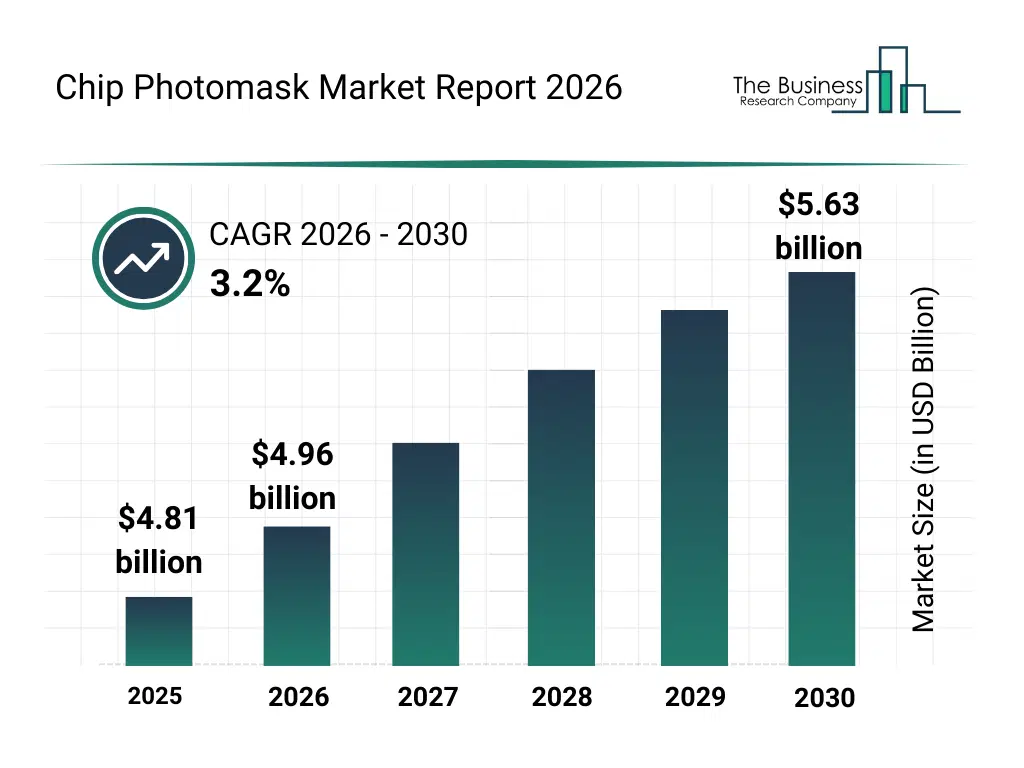
What Is The Chip Photomask Market Size 2026 And Growth Rate?
The chip photomask market size has grown steadily in recent years. It will grow from $4.81 billion in 2025 to $4.96 billion in 2026 at a compound annual growth rate (CAGR) of 3.1%. The growth in the historic period can be attributed to increasing demand for integrated circuits, adoption of conventional photomasks, growth in consumer electronics, expansion of semiconductor fabs in asia, improvement in lithography accuracy.What Is The Chip Photomask Market Growth Forecast?
The chip photomask market size is expected to see steady growth in the next few years. It will grow to $5.63 billion in 2030 at a compound annual growth rate (CAGR) of 3.2%. The growth in the forecast period can be attributed to rising adoption of euv photomasks, increasing ic complexity, investment in smart manufacturing, expansion of semiconductor foundries in north america and europe, innovation in mask materials and coatings. Major trends in the forecast period include miniaturization of ics, advanced photolithography techniques, high-precision mask fabrication, euv and duv lithography adoption, automation in semiconductor production.
Global Chip Photomask Market Segmentation
1) By Type: Binary Photomasks, Phase-Shifting Photomasks, Chromeless Photomasks, Other Types 2) By Application: Semiconductor Manufacturing, Flat Panel Display Manufacturing, Micro-Electromechanical Systems (MEMS), Other Applications 3) By End-Use Industry: Consumer Electronics, Automotive, Telecommunications, Healthcare Subsegments: 1) By Binary Photomasks: Conventional Binary Photomasks, Optical Enhancements Binary Photomasks, High-Resolution Binary Photomasks, Deep UV (DUV) Binary Photomasks 2) By Phase-Shifting Photomasks: Alternating Phase-Shifting Photomasks (Alt-PSM), Attenuated Phase-Shifting Photomasks (Att-PSM), Rim-Shifting Phase Photomasks, Sub-Wavelength Phase-Shifting Photomasks 3) By Chromeless Photomasks: Scattering-Based Chromeless Photomasks, Interference-Based Chromeless Photomasks, Advanced Lithography Chromeless Photomasks, Extreme UV (EUV) Chromeless Photomasks 4) By Other Types: EUV (Extreme Ultraviolet) Photomasks, Nano-Imprint Lithography Photomasks, Multi-Layer Mask Photomasks, Hybrid PhotomasksWhat Is The Driver Of The Chip Photomask Market?
The growth in consumer electronics is expected to propel the growth of the chip photomask market going forward. Consumer electronics are devices designed for everyday personal and household use, such as smartphones, laptops, TVs, and home appliances. Growth in consumer electronics is driven by several factors, including rising disposable income, expansion of 5G networks, e-commerce growth, and e-learning trends. Chip photomasks enable the production of smaller, more efficient, and more powerful semiconductor chips, supporting the growing demand for advanced consumer electronics with enhanced performance and energy efficiency. For instance, in May 2023, according to the Japan Electronics and Information Technology Industries Association, a Japan-based trade association, the total consumer electronics production reached $279.01 million (¥32,099 million) in May 2023, compared to $219.64 million (¥25,268 million) in May 2022. Therefore, the growth in consumer electronics drives the growth of the chip photomask industry.Key Players In The Global Chip Photomask Market
Major companies operating in the chip photomask market are Applied Materials, ASML Holding N.V., DAI Nippon Printing Co. Ltd., Semiconductor Manufacturing International Corporation, Synopsys Inc., Hoya Corporation, Nikon Corporation, Benchmark Technologies, Hua Hong Semiconductor Limited, Photronics Inc., Lasertec Corporation, SUSS MicroTec, Taiwan Mask Corporation, Shenzhen Qingyi Photomask Limited, Laserlab, Inc., Heidelberg Instruments, HTA Photomask, Martin Photomask Services, Tekscend Photomask, Mutech Microsystems.
This chart is for illustrative purposes; the full report includes a detailed competitor analysis and comprehensive overview of the top 10 companies in the market.
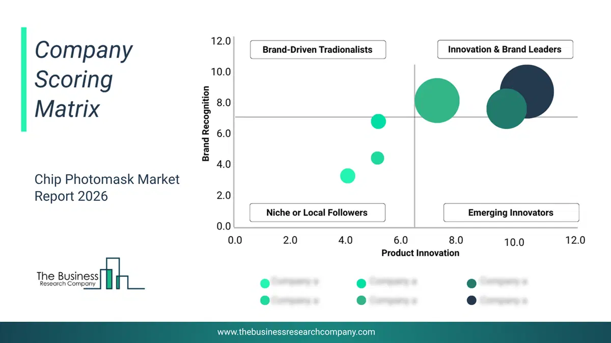
This chart maps companies by product innovation and brand strength, with bubble size indicating relative revenue, helping identify market leaders, challengers, and niche players. This is an illustrative chart; the full report provides a complete and accurate competitive analysis.
Global Chip Photomask Market Trends and Insights
Major companies operating in the chip photomask market are focusing on adopting a strategic partnership approach to develop advanced chip-based technology. A strategic partnership is a collaborative agreement between two or more organizations to combine strengths, resources, or expertise for mutual benefit while remaining independent. For instance, in November 2024, Tekscend Photomask Germany GmbH, a Germany-based provider of photomasks for semiconductors, partnered with Advanced Mask Technology Center (AMTC), a Germany-based developer and producer of photolithography masks, to unveil Europe's first MBMW-100 Flex, a multibeam mask writer. This innovative tool significantly reduces mask writing time for complex semiconductor designs from multiple days to just 7-12 hours, enhancing Europe's semiconductor capabilities and competitiveness in advanced chip technology.What Are Latest Mergers And Acquisitions In The Chip Photomask Market?
In February 2025, Toppan Photomask, a US-based semiconductor manufacturing company, entered a partnership with IBM. The aim of the partnership between Toppan Photomask and IBM is to develop advanced photomask capabilities for 2-nanometer (nm) logic semiconductor nodes and beyond, using extreme ultraviolet (EUV) lithography and High-NA EUV technology. IBM is a US-based technology company that manufactures chip photomasks.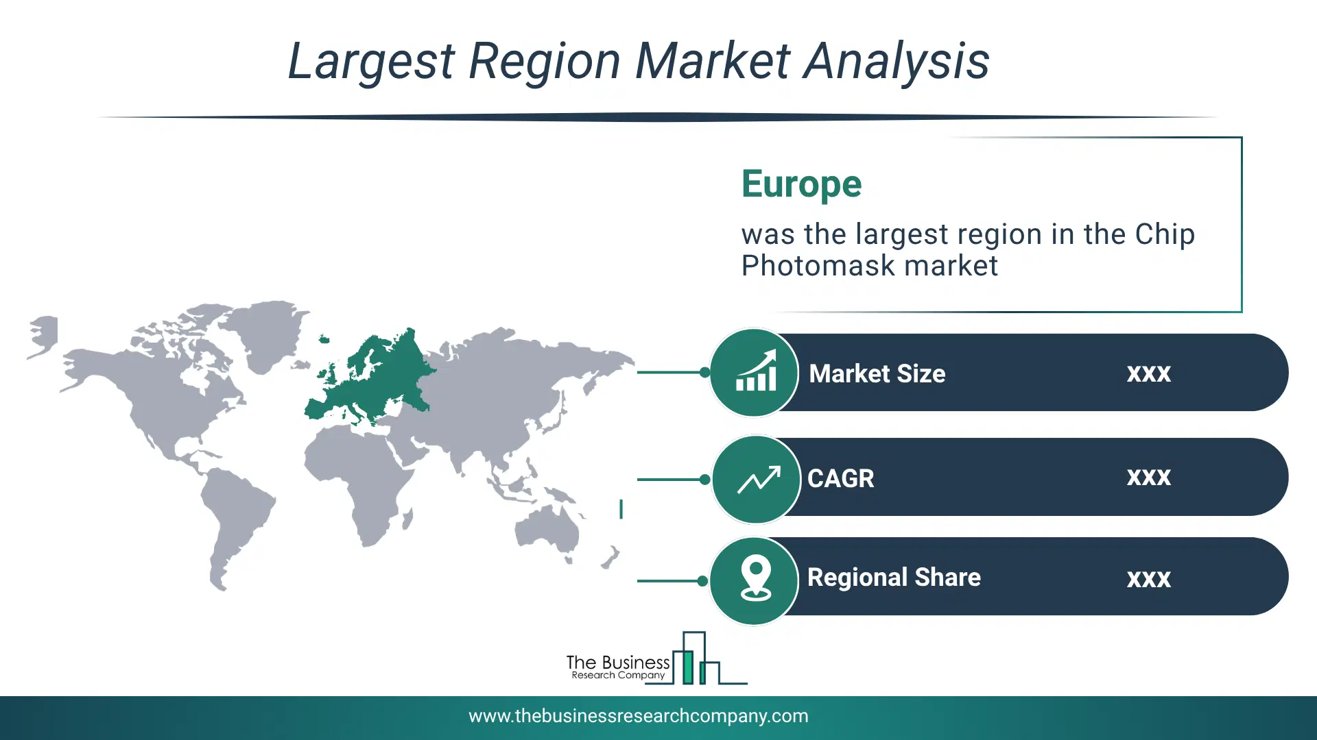
Regional Outlook
Europe was the largest region in the chip photomask market in 2025. Asia-Pacific is expected to be the fastest-growing region in the forecast period. The regions covered in this market report are Asia-Pacific, South East Asia, Western Europe, Eastern Europe, North America, South America, Middle East, Africa. The countries covered in this market report are Australia, Brazil, China, France, Germany, India, Indonesia, Japan, Taiwan, Russia, South Korea, UK, USA, Canada, Italy, Spain.What Defines the Chip Photomask Market?
The chip photomask market consists of sales of multi-layer masks (MLM), alternating phase shift masks (alternating PSM), and optical proximity correction masks. Values in this market are ‘factory gate’ values, that is the value of goods sold by the manufacturers or creators of the goods, whether to other entities (including downstream manufacturers, wholesalers, distributors and retailers) or directly to end customers. The value of goods in this market includes related services sold by the creators of the goods.How is Market Value Defined and Measured?
The market value is defined as the revenues that enterprises gain from the sale of goods and/or services within the specified market and geography through sales, grants, or donations in terms of the currency (in USD unless otherwise specified). The revenues for a specified geography are consumption values that are revenues generated by organizations in the specified geography within the market, irrespective of where they are produced. It does not include revenues from resales along the supply chain, either further along the supply chain or as part of other products.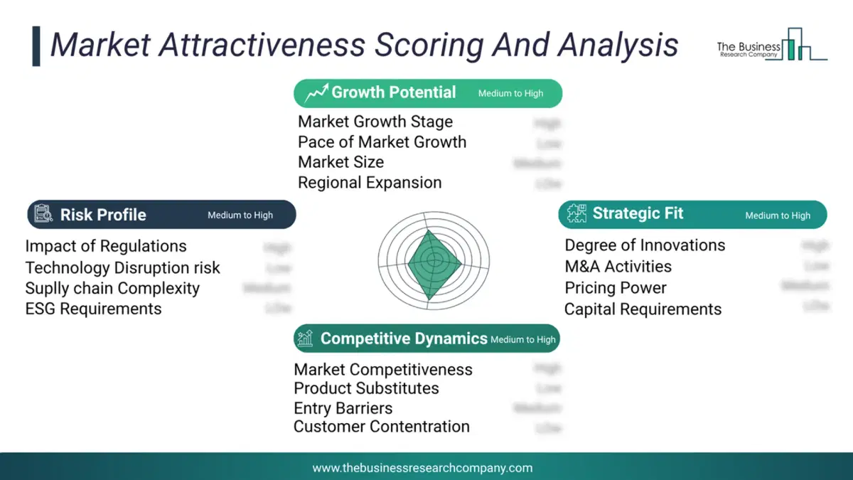
This chart presents market attractiveness based on a quantitative evaluation of growth, competition, strategic alignment, and risk, offering a clear view of opportunity areas for decision-making. This chart is for illustrative purposes; the full report contains the complete analysis.
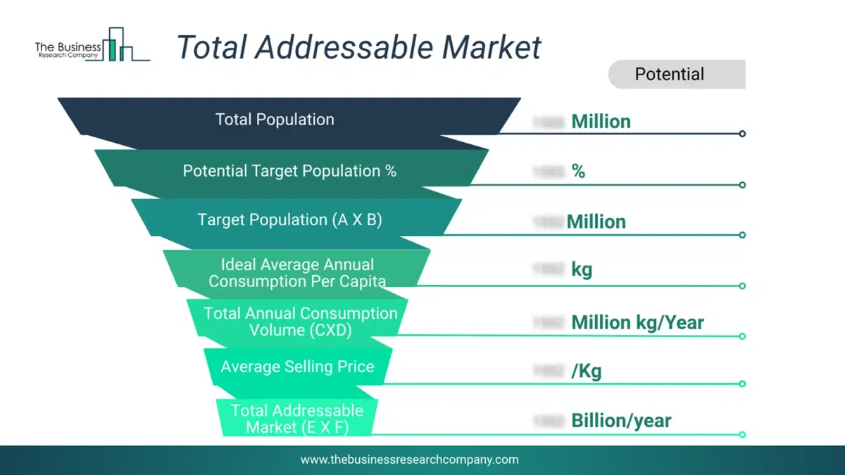
This chart highlights the Total Addressable Market (TAM) by estimating the maximum revenue opportunity using an assumption-driven approach, supporting strategic planning and opportunity sizing across markets. The chart is illustrative; the full report provides a more comprehensive analysis.
What Key Data and Analysis Are Included in the Chip Photomask Market Report 2026?
The chip photomask market research report is one of a series of new reports from The Business Research Company that provides market statistics, including industry global market size, regional shares, competitors with the market share, detailed market segments, market trends and opportunities, and any further data you may need to thrive in the chip photomask industry. The market research report delivers a complete perspective of everything you need, with an in-depth analysis of the current and future state of the industry.Chip Photomask Market Report Forecast Analysis
| Report Attribute | Details |
|---|---|
| Market Size Value In 2026 | $4.96 billion |
| Revenue Forecast In 2030 | $5.63 billion |
| Growth Rate | CAGR of 3.2% from 2026 to 2030 |
| Base Year For Estimation | 2025 |
| Actual Estimates/Historical Data | 2020-2025 |
| Forecast Period | 2026 - 2030 |
| Market Representation | Revenue in USD Billion and CAGR from 2026 to 2030 |
| Segments Covered | Type, Application, End-Use Industry |
| Regional Scope | Asia-Pacific, Western Europe, Eastern Europe, North America, South America, Middle East, Africa |
| Country Scope | The countries covered in the report are Australia, Brazil, China, France, Germany, India, Indonesia, Japan, Taiwan, Russia, South Korea, UK, USA, Canada, Italy, Spain. |
| Key Companies Profiled | Applied Materials, ASML Holding N.V., DAI Nippon Printing Co. Ltd., Semiconductor Manufacturing International Corporation, Synopsys Inc., Hoya Corporation, Nikon Corporation, Benchmark Technologies, Hua Hong Semiconductor Limited, Photronics Inc., Lasertec Corporation, SUSS MicroTec, Taiwan Mask Corporation, Shenzhen Qingyi Photomask Limited, Laserlab, Inc., Heidelberg Instruments, HTA Photomask, Martin Photomask Services, Tekscend Photomask, Mutech Microsystems. |
| Customization Scope | Request for Customization |
| Pricing And Purchase Options | Explore Purchase Options |