
Fin Field Effect Transistor (FinFET) Wafer Foundry Market Report 2026
Global Outlook – By Product Type (Central Processing Unit, Field Programmable Gate Array, Graphics Processing Unit, System On Chip, Microcontroller Unit, Network Processors, Other Types), By Fin Field Effect Transistor Process Node (14 Nanometer Fin Field Effect Transistor Technology, 7 Nanometer Fin Field Effect Transistor Technology, 5 Nanometer Fin Field Effect Transistor Technology, 3 Nanometer Fin Field Effect Transistor Technology), By Technology Type (Bulk Fin Field Effect Transistor, Silicon On Insulator Fin Field Effect Transistor, Fully Depleted Silicon On Insulator Fin Field Effect Transistor), By End User Industry (Telecommunications, Automotive, Consumer Electronics, Industrial Electronics, Healthcare Devices) – Market Size, Trends, Strategies, and Forecast to 2030
Fin Field Effect Transistor (FinFET) Wafer Foundry Market Overview
• Fin Field Effect Transistor (FinFET) Wafer Foundry market size has reached to $53.93 billion in 2025 • Expected to grow to $80.34 billion in 2030 at a compound annual growth rate (CAGR) of 8.2% • Growth Driver: Rising Demand for Artificial Intelligence Chips Is Fueling the Growth of the Market Due to Increasing Adoption of Generative Artificial Intelligence Applications • Market Trend: Advancements In Fin Field-Effect Transistor Process Technologies Enhancing Semiconductor Performance And Efficiency • North America was the largest region in 2025 and Asia-Pacific is the fastest growing region.What Is Covered Under Fin Field Effect Transistor (FinFET) Wafer Foundry Market?
Fin field effect transistor (FinFET) wafer foundry refers to contract semiconductor manufacturing services that fabricate integrated circuits using fin field effect transistor (FinFET) process technology. FinFET technology employs three-dimensional transistor structures to improve performance, reduce power consumption, and increase transistor density, making it suitable for advanced applications such as artificial intelligence, high-performance computing, mobile processors, automotive electronics, networking, and data centers. The main product types of fin field effect transistor (FinFET) wafer foundry include central processing units, field programmable gate arrays, graphics processing units, system on chips, microcontroller units, network processors, and other types. Central processing units refer to semiconductor processors that execute instructions and perform general-purpose computing functions within electronic systems. These products are manufactured using 14 nanometer Fin Field Effect Transistor technology, 7 nanometer Fin Field Effect Transistor technology, 5 nanometer Fin Field Effect Transistor technology, and 3 nanometer Fin Field Effect Transistor technology. They use bulk Fin Field Effect Transistor, silicon on insulator Fin Field Effect Transistor, and fully depleted silicon on insulator Fin Field Effect Transistor technologies and serve end user industries across telecommunications, automotive, consumer electronics, industrial electronics, and healthcare devices.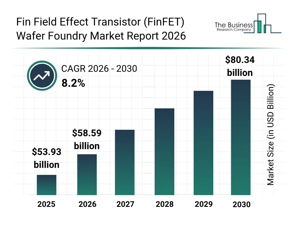
What Is The Fin Field Effect Transistor (FinFET) Wafer Foundry Market Size and Share 2026?
The fin field effect transistor (finfet) wafer foundry market size has grown strongly in recent years. It will grow from $53.93 billion in 2025 to $58.59 billion in 2026 at a compound annual growth rate (CAGR) of 8.6%. The growth in the historic period can be attributed to growth in semiconductor demand, increasing adoption of smartphones and mobile processors, expansion of data center infrastructure, rising demand for advanced processors, growth in automotive electronics.What Is The Fin Field Effect Transistor (FinFET) Wafer Foundry Market Growth Forecast?
The fin field effect transistor (finfet) wafer foundry market size is expected to see strong growth in the next few years. It will grow to $80.34 billion in 2030 at a compound annual growth rate (CAGR) of 8.2%. The growth in the forecast period can be attributed to increasing AI accelerator demand, rising high-performance computing requirements, expansion of advanced-node semiconductor manufacturing, growing demand for automotive SoCs, increasing semiconductor content in connected devices. Major trends in the forecast period include increasing adoption of advanced FinFET process nodes, growing demand for high-performance semiconductor manufacturing, rising investment in advanced foundry capacity, increasing demand for customized semiconductor fabrication, growing adoption of 3D transistor architectures.
Global Fin Field Effect Transistor (FinFET) Wafer Foundry Market Segmentation
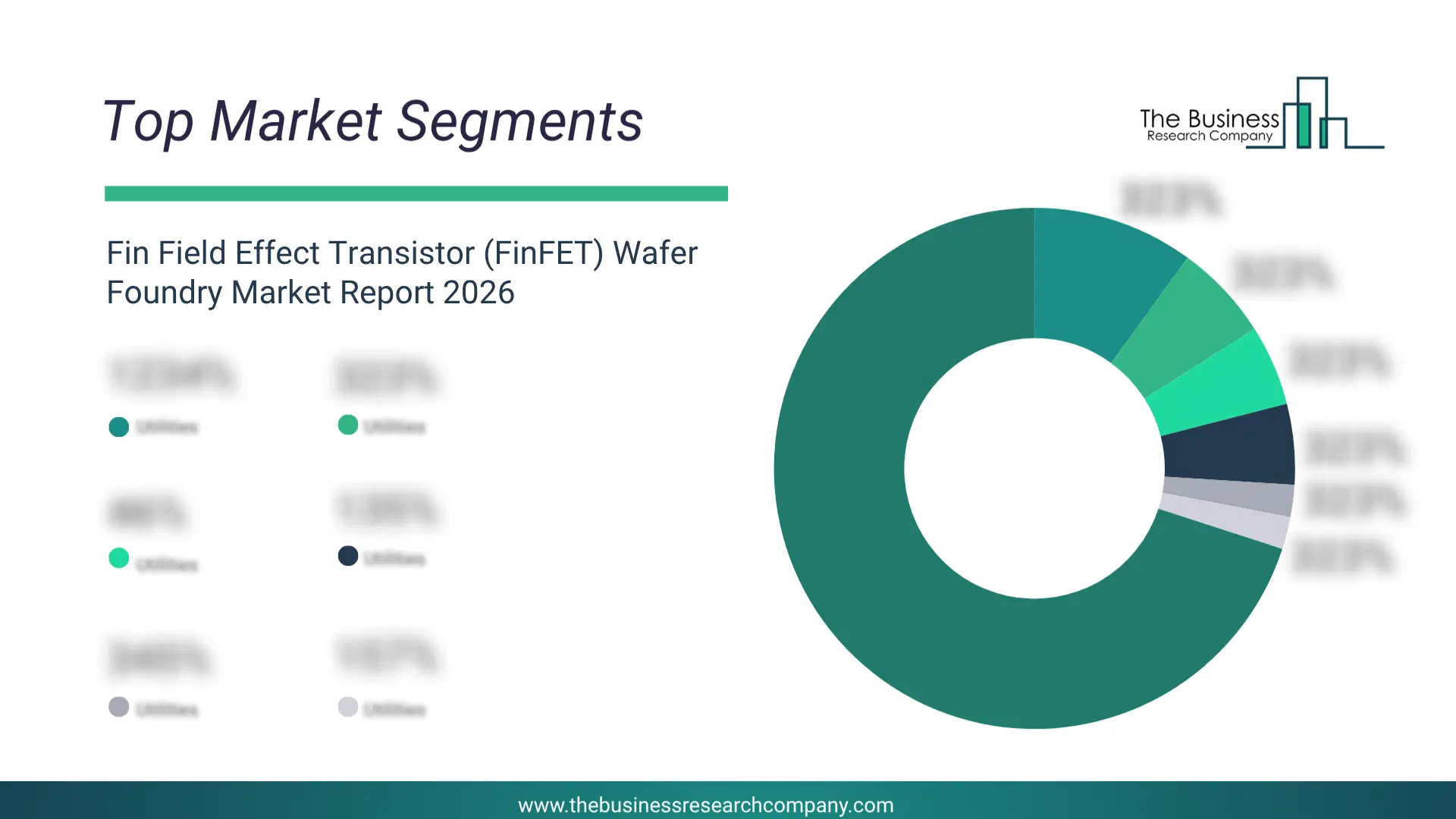
1) By Product Type: Central Processing Unit, Field Programmable Gate Array, Graphics Processing Unit, System On Chip, Microcontroller Unit, Network Processors, Other Types 2) By Fin Field Effect Transistor Process Node: 14 Nanometer Fin Field Effect Transistor Technology, 7 Nanometer Fin Field Effect Transistor Technology, 5 Nanometer Fin Field Effect Transistor Technology, 3 Nanometer Fin Field Effect Transistor Technology 3) By Technology Type: Bulk Fin Field Effect Transistor, Silicon On Insulator Fin Field Effect Transistor, Fully Depleted Silicon On Insulator Fin Field Effect Transistor 4) By End User Industry: Telecommunications, Automotive, Consumer Electronics, Industrial Electronics, Healthcare Devices Subsegments: 1) By Central Processing Unit: Desktop Processor, Mobile Processor, Server Processor, Embedded Processor 2) By Field Programmable Gate Array: Low Density Field Programmable Gate Array, Mid Density Field Programmable Gate Array, High Density Field Programmable Gate Array, System On Module Field Programmable Gate Array 3) By Graphics Processing Unit: Integrated Graphics Processing Unit, Discrete Graphics Processing Unit, Data Center Graphics Processing Unit, Embedded Graphics Processing Unit 4) By System On Chip: Mobile System On Chip, Automotive System On Chip, Industrial System On Chip, Internet Of Things System On Chip 5) By Microcontroller Unit: Eight Bit Microcontroller Unit, Sixteen Bit Microcontroller Unit, Thirty Two Bit Microcontroller Unit, Automotive Microcontroller Unit 6) By Network Processors: Multi Core Network Processor, Packet Processing Network Processor, Communication Network Processor, Security Network Processor 7) By Other Types: Artificial Intelligence Accelerators, Digital Signal Processors, Application Specific Integrated Circuits, Security ProcessorsWhat Is The Driver Of The Fin Field Effect Transistor (FinFET) Wafer Foundry Market?
The rising demand for artificial intelligence chips is expected to propel the growth of the fin field effect transistor (FinFET) wafer foundry market going forward. Artificial intelligence chips are specialized semiconductor devices designed to accelerate AI workloads such as machine learning, deep learning, and neural network processing with high computational efficiency. Artificial intelligence chips are experiencing rising demand due to the increasing adoption of generative artificial intelligence applications. The rising demand for artificial intelligence chips increases the need for FinFET wafer foundry services as AI processors require advanced FinFET transistor architectures to deliver high computing performance, improved power efficiency, and greater transistor density for complex AI workloads. For instance, in June 2026, according to the Semiconductor Industry Association (SIA), a US-based semiconductor industry association, semiconductors accounted for more than 95% of the content value of a leading artificial intelligence (AI) data server rack, with each AI server rack containing over 4,500 packaged chips. Therefore, the rising demand for artificial intelligence chips is driving the growth of the fin field effect transistor (FinFET) wafer foundry industry.Key Players In The Global Fin Field Effect Transistor (FinFET) Wafer Foundry Market
Major companies operating in the fin field effect transistor (finfet) wafer foundry market are Taiwan Semiconductor Manufacturing Company Limited, Samsung Electronics Co. Ltd., Intel Corporation, United Microelectronics Corporation, GlobalFoundries Inc., Semiconductor Manufacturing International Corporation, Shanghai Huali Microelectronics Corporation, Sony Semiconductor Solutions Corporation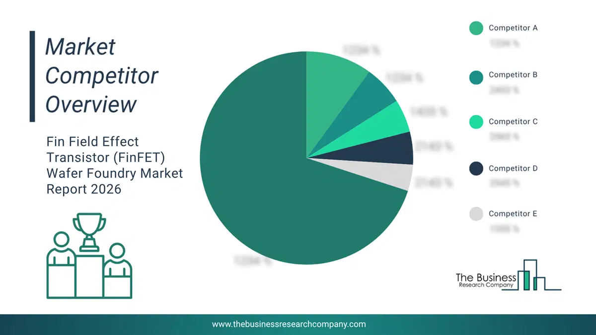
This chart is for illustrative purposes; the full report includes a detailed competitor analysis and comprehensive overview of the top 10 companies in the market.
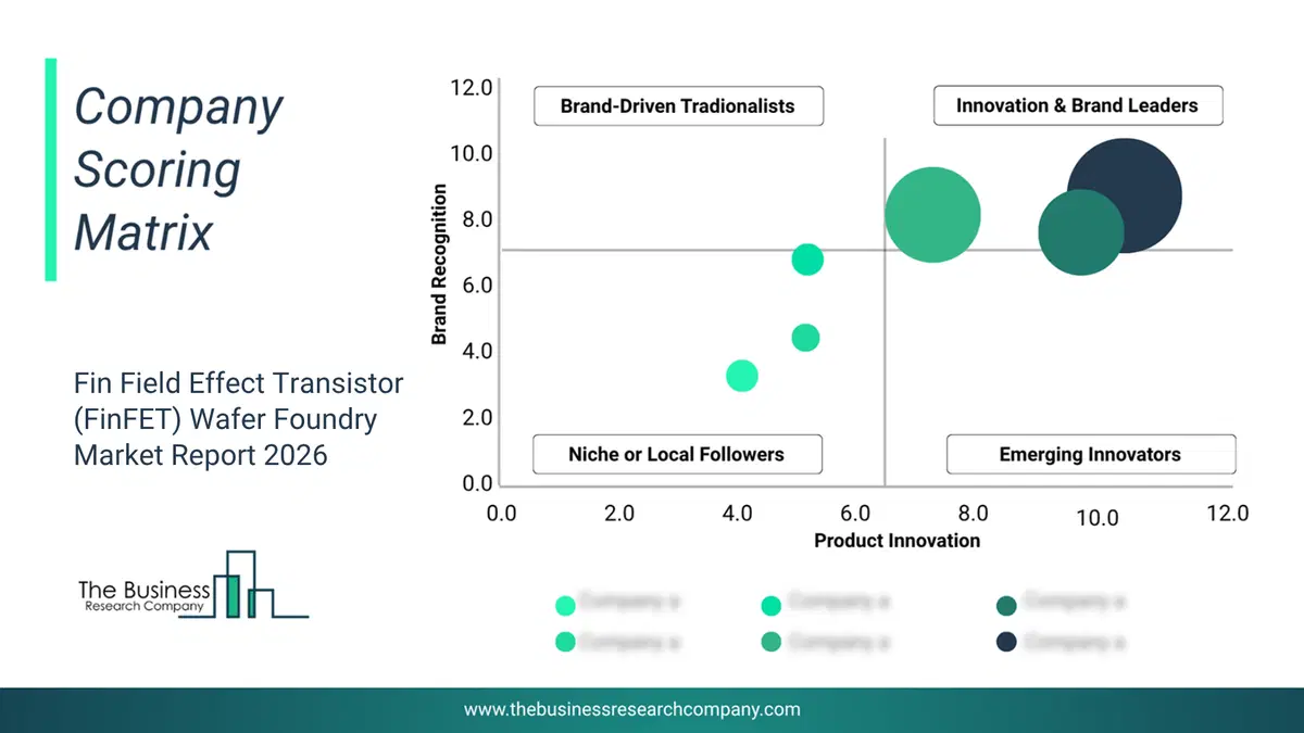
This chart maps companies by product innovation and brand strength, with bubble size indicating relative revenue, helping identify market leaders, challengers, and niche players. This is an illustrative chart; the full report provides a complete and accurate competitive analysis.
Global Fin Field Effect Transistor (FinFET) Wafer Foundry Market Trends and Insights
Major companies operating in the fin field effect transistor (FinFET) wafer foundry market are focusing on developing innovative solutions, such as fin field effect transistor process technologies, to enhance transistor performance, reduce power consumption, improve chip density, and support the increasing demand for advanced semiconductor manufacturing in artificial intelligence, high-performance computing, automotive electronics, and mobile applications. FinFET process technologies are advanced semiconductor fabrication methods that use three-dimensional fin-shaped transistor structures to provide better control over current flow compared with traditional planar transistors, enabling higher performance and energy efficiency at smaller process nodes. For instance, in May 2026, United Microelectronics Corporation (UMC), a Taiwan-based semiconductor foundry company, launched its 14nm embedded high-voltage (eHV) FinFET technology platform, an advanced wafer fabrication solution designed for next-generation display driver integrated circuits (ICs). The platform is based on Fin Field-Effect Transistor (FinFET) process technology, which uses three-dimensional transistor structures to improve power efficiency, performance, and transistor density compared with traditional planar transistor technologies. Validated at UMC’s Fab 12A, the technology enables semiconductor manufacturers to develop smaller, more power-efficient, and higher-performance display driver ICs for advanced display applications. The platform provides enhanced electrical performance and reduced chip size while supporting the growing demand for high-resolution smartphone displays and next-generation display technologies. By offering a validated FinFET-based manufacturing process with an available process design kit (PDK), UMC enables customers to accelerate the development and production of advanced semiconductor devices.What Are Latest Mergers And Acquisitions In The Fin Field Effect Transistor (FinFET) Wafer Foundry Market?
In January 2024, Intel Corporation, a US-based technology company, partnered with United Microelectronics Corporation (UMC) to develop a 12-nanometer semiconductor process platform for high-growth markets. Through this collaboration, Intel and UMC aim to provide a U.S.-manufactured 12-nanometer process with Fin Field Effect Transistor (FinFET) capabilities by leveraging Intel’s high-volume manufacturing capacity and FinFET transistor design expertise, along with UMC’s foundry process experience and design support capabilities. United Microelectronics Corporation (UMC) is a Taiwan-based provider of Fin Field Effect Transistor (FinFET) wafer foundry services.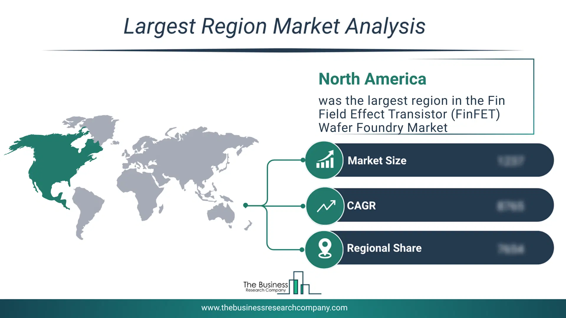
Regional Outlook
North America was the largest region in the fin field effect transistor (finfet) wafer foundry market in 2025. Asia-Pacific is expected to be the fastest-growing region in the forecast period. The regions covered in this market report are Asia-Pacific, South East Asia, Western Europe, Eastern Europe, North America, South America, Middle East, Africa. The countries covered in this market report are Australia, Brazil, China, France, Germany, India, Indonesia, Japan, Taiwan, Russia, South Korea, UK, USA, Canada, Italy, Spain.What Defines the Fin Field Effect Transistor (FinFET) Wafer Foundry Market?
The fin field effect transistor (FinFET) wafer foundry market includes revenues earned by entities by providing services such as wafer fabrication services, FinFET process manufacturing, advanced process node production, prototype chip fabrication, volume semiconductor manufacturing, process development, yield optimization, and related semiconductor manufacturing services. The market value includes the value of related goods sold by the service provider or included within the service offering. Only goods and services traded between entities or sold to end consumers are included.How is Market Value Defined and Measured?
The market value is defined as the revenues that enterprises gain from the sale of goods and/or services within the specified market and geography through sales, grants, or donations in terms of the currency (in USD unless otherwise specified). The revenues for a specified geography are consumption values that are revenues generated by organizations in the specified geography within the market, irrespective of where they are produced. It does not include revenues from resales along the supply chain, either further along the supply chain or as part of other products.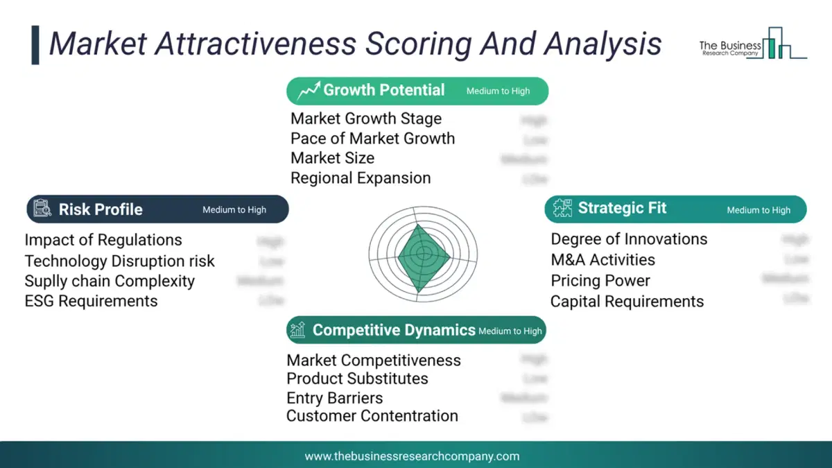
This chart presents market attractiveness based on a quantitative evaluation of growth, competition, strategic alignment, and risk, offering a clear view of opportunity areas for decision-making. This chart is for illustrative purposes; the full report contains the complete analysis.
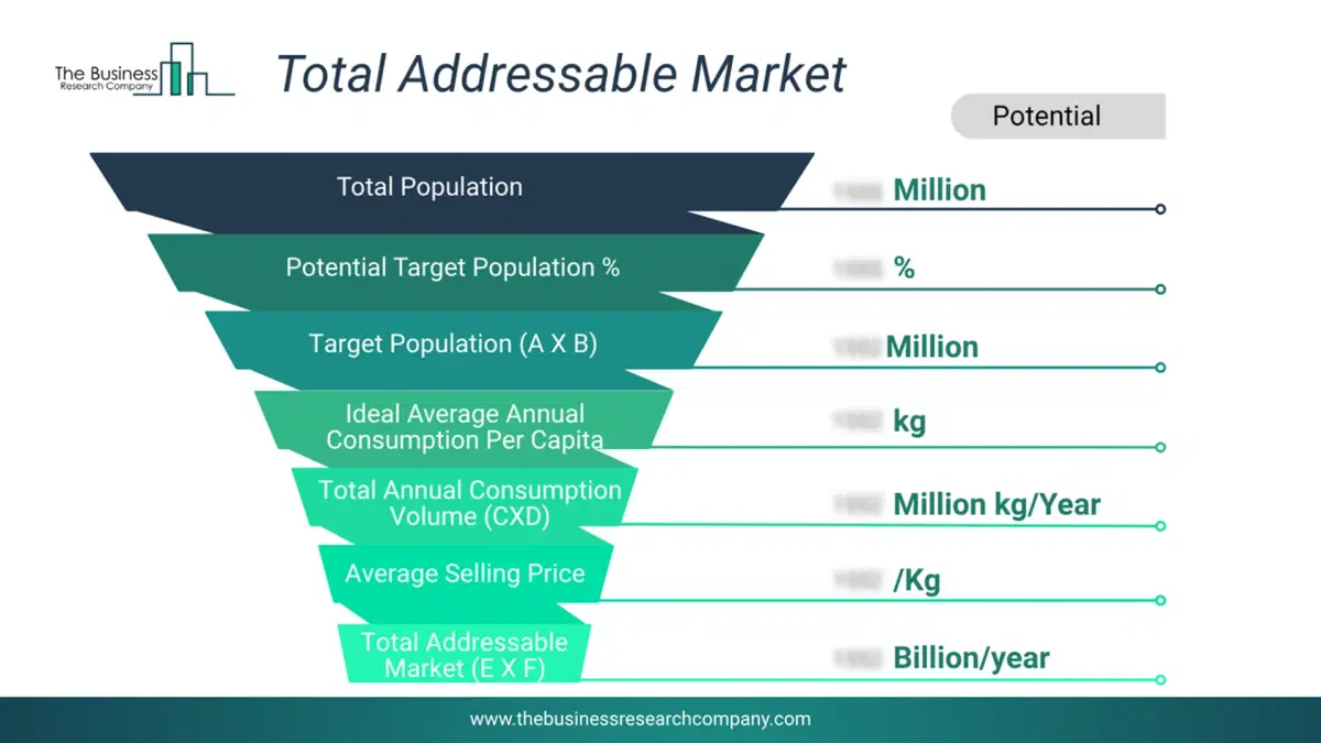
This chart highlights the Total Addressable Market (TAM) by estimating the maximum revenue opportunity using an assumption-driven approach, supporting strategic planning and opportunity sizing across markets. The chart is illustrative; the full report provides a more comprehensive analysis.
What Key Data and Analysis Are Included in the Fin Field Effect Transistor (FinFET) Wafer Foundry Market Report 2026?
The fin field effect transistor (finfet) wafer foundry market research report is one of a series of new reports from The Business Research Company that provides market statistics, including industry global market size, regional shares, competitors with the market share, detailed market segments, market trends and opportunities, and any further data you may need to thrive in the fin field effect transistor (finfet) wafer foundry industry. The market research report delivers a complete perspective of everything you need, with an in-depth analysis of the current and future state of the industry.Fin Field Effect Transistor (FinFET) Wafer Foundry Market Report Forecast Analysis
| Report Attribute | Details |
|---|---|
| Market Size Value In 2026 | $58.59 billion |
| Revenue Forecast In 2030 | $80.34 billion |
| Growth Rate | CAGR of 8.2% from 2026 to 2030 |
| Base Year For Estimation | 2025 |
| Actual Estimates/Historical Data | 2020-2025 |
| Forecast Period | 2026 - 2030 |
| Market Representation | Revenue in USD Billion and CAGR from 2026 to 2030 |
| Segments Covered | Product Type, Fin Field Effect Transistor Process Node, Technology Type, End User Industry |
| Regional Scope | Asia-Pacific, Western Europe, Eastern Europe, North America, South America, Middle East, Africa |
| Country Scope | The countries covered in the report are Australia, Brazil, China, France, Germany, India, Indonesia, Japan, Taiwan, Russia, South Korea, UK, USA, Canada, Italy, Spain. |
| Key Companies Profiled | Taiwan Semiconductor Manufacturing Company Limited, Samsung Electronics Co. Ltd., Intel Corporation, United Microelectronics Corporation, GlobalFoundries Inc., Semiconductor Manufacturing International Corporation, Shanghai Huali Microelectronics Corporation, Sony Semiconductor Solutions Corporation |
| Customization Scope | Request for Customization |
| Pricing And Purchase Options | Explore Purchase Options |