

Flip Chip Bonder Market Report 2026
Global Outlook – By Type (Fully Automatic Flip Chip Bonders, Semi-Automatic Flip Chip Bonders, Manual Flip Chip Bonders), By Technology (Thermocompression Bonding, Thermosonic Bonding, Fluxless Bonding, Adhesive Bonding), By Packaging Type (Two-Dimensional Packaging, Two-And-A-Half-Dimensional Packaging, Three-Dimensional Integrated Circuit Packaging, Wafer-Level Packaging), By Application (Consumer Electronics, Automotive Electronics, Telecommunications, Data Centers And High-Performance Computing, Industrial Electronics, Aerospace And Defense), By End User (Semiconductor Foundries, Outsourced Semiconductor Assembly And Test Companies, Integrated Device Manufacturers, Research And Development Labs) – Market Size, Trends, Strategies, and Forecast to 2035
Flip Chip Bonder Market Overview
• Flip Chip Bonder market size has reached to $0.5 billion in 2025 • Expected to grow to $0.75 billion in 2030 at a compound annual growth rate (CAGR) of 8.1% • Growth Driver: Expansion of 5G Communication Infrastructure Driving The Market Growth Due To Increasing Demand For Miniaturized Semiconductor Components • Market Trend: Large-Die Handling Expands Advanced Packaging Capabilities • Asia-Pacific was the largest region and fastest growing region.What Is Covered Under Flip Chip Bonder Market?
Flip chip bonders refer to specialized semiconductor assembly equipment used to attach semiconductor dies directly onto substrates or packages by forming electrical and mechanical connections through solder bumps, copper pillars, or other interconnect technologies. These machines enable high-precision placement, alignment, and bonding of microelectronic components, supporting advanced packaging technologies that improve performance, miniaturization, and reliability of semiconductor devices. The main types of flip chip bonders include fully automatic flip chip bonders, semi-automatic flip chip bonders, and manual flip chip bonders. Fully automatic flip chip bonders refer to advanced equipment that automates chip alignment, placement, bonding, and related assembly operations to improve precision and production efficiency. These systems use thermocompression bonding, thermosonic bonding, fluxless bonding, and adhesive bonding technologies and support two-dimensional packaging, two-and-a-half-dimensional packaging, three-dimensional integrated circuit packaging, and wafer-level packaging. The various applications involved are consumer electronics, automotive electronics, telecommunications, data centers and high-performance computing, industrial electronics, and aerospace and defense, and they are used by several end users such as semiconductor foundries, outsourced semiconductor assembly and test companies, integrated device manufacturers, and research and development labs.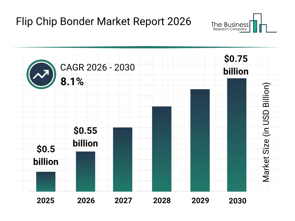
What Is The Flip Chip Bonder Market Size and Share 2026?
The flip chip bonder market size has grown strongly in recent years. It will grow from $0.5 billion in 2025 to $0.55 billion in 2026 at a compound annual growth rate (CAGR) of 9.7%. The growth in the historic period can be attributed to increasing demand for advanced semiconductor packaging, rising adoption of flip chip assembly in consumer electronics, growing need for miniaturized semiconductor devices, increasing use of high-density interconnect technologies, rising semiconductor production requiring automated die bonding equipment.What Is The Flip Chip Bonder Market Growth Forecast?
The flip chip bonder market size is expected to see strong growth in the next few years. It will grow to $0.75 billion in 2030 at a compound annual growth rate (CAGR) of 8.1%. The growth in the forecast period can be attributed to expanding demand for high-performance computing and data center semiconductors, increasing adoption of advanced packaging for AI processors, growing need for high-speed and high-precision semiconductor assembly, rising production of automotive electronic components requiring advanced packaging, increasing demand for 3D IC and wafer-level packaging equipment. Major trends in the forecast period include increasing adoption of fully automatic flip chip bonders for high-volume semiconductor assembly, rising demand for thermocompression bonding to support fine-pitch semiconductor interconnections, growing use of wafer-level packaging to improve semiconductor manufacturing efficiency and device miniaturization, increasing preference for high-precision die placement to support advanced semiconductor packaging requirements, expanding adoption of three-dimensional packaging for higher interconnect density and improved device performance.Tariff Impact On Flip Chip Bonder Market
Tariffs are impacting the flip chip bonders market by increasing the cost of imported semiconductor assembly equipment, precision positioning components, bonding tools, electronic control systems, and specialized machinery required for advanced chip packaging. This is raising equipment procurement and manufacturing costs for semiconductor producers, particularly in regions dependent on imported semiconductor equipment such as Asia-Pacific and other major electronics manufacturing hubs. Capital-intensive segments such as fully automatic flip chip bonders and advanced packaging applications are most affected due to global equipment and component supply chain dependencies. However, tariffs are also encouraging domestic semiconductor equipment manufacturing, regional supplier diversification, localized component sourcing, and increased investment in domestic semiconductor packaging ecosystems, creating greater long-term supply chain resilience.
Global Flip Chip Bonder Market Segmentation
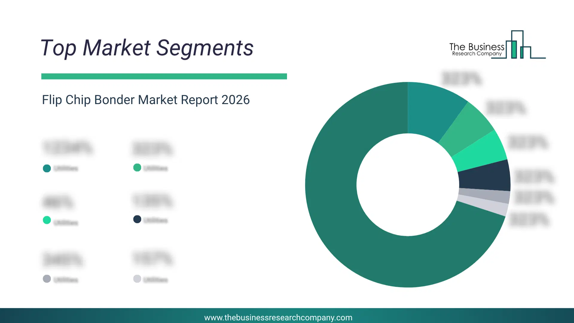
2) By Technology: Thermocompression Bonding, Thermosonic Bonding, Fluxless Bonding, Adhesive Bonding 3) By Packaging Type: Two-Dimensional Packaging, Two-And-A-Half-Dimensional Packaging, Three-Dimensional Integrated Circuit Packaging, Wafer-Level Packaging 4) By Application: Consumer Electronics, Automotive Electronics, Telecommunications, Data Centers And High-Performance Computing, Industrial Electronics, Aerospace And Defense 5) By End User: Semiconductor Foundries, Outsourced Semiconductor Assembly And Test Companies, Integrated Device Manufacturers, Research And Development Labs Subsegments: 1) By Fully Automatic Flip Chip Bonders: High Precision Fully Automatic Flip Chip Bonders, High Speed Fully Automatic Flip Chip Bonders, Advanced Packaging Fully Automatic Flip Chip Bonders, Wafer Level Fully Automatic Flip Chip Bonders, Three Dimensional Fully Automatic Flip Chip Bonders 2) By Semi-Automatic Flip Chip Bonders: Precision Semi-Automatic Flip Chip Bonders, Research And Development Semi-Automatic Flip Chip Bonders, Small Batch Semi-Automatic Flip Chip Bonders, Wafer Level Semi-Automatic Flip Chip Bonders, Advanced Assembly Semi-Automatic Flip Chip Bonders 3) By Manual Flip Chip Bonders: Laboratory Manual Flip Chip Bonders, Prototype Manual Flip Chip Bonders, Small Scale Manual Flip Chip Bonders, Research Manual Flip Chip Bonders, Educational Manual Flip Chip BondersWhat Is The Driver Of The Flip Chip Bonder Market?
The expansion of 5G communication infrastructure is expected to propel the growth of the flip chip bonder market going forward. 5G communication infrastructure refers to the advanced network ecosystem comprising base stations, antennas, radio access networks, and semiconductor components that enable high-speed data transmission, low latency, and enhanced connectivity. The demand for 5G infrastructure is increasing due to the rapid adoption of connected devices, as the growing number of smartphones, Internet of Things (IoT) devices, autonomous systems, and smart technologies requires faster data transmission. The expansion of 5G communication infrastructure drives demand for flip chip bonders by increasing the need for high-precision semiconductor packaging technologies that support miniaturization, improved thermal performance, higher input/output density, and enhanced reliability of advanced chips used in 5G applications. For instance, in October 2025, according to the International Telecommunication Union (ITU), a Switzerland-based United Nations specialized agency, 66% of the world's urban population and 40% of its rural population were covered by 5G networks in 2025. Therefore, the expansion of 5G communication infrastructure is driving the growth of the flip chip bonder industry.Key Players In The Global Flip Chip Bonder Market
Major companies operating in the flip chip bonder market are ASMPT Limited, Panasonic Holdings Corporation, Yamaha Motor Co. Ltd., BE Semiconductor Industries N.V., Kulicke & Soffa Industries Inc., Hanmi Semiconductor Co. Ltd., Hanwha Semitech Co. Ltd., Toray Engineering Co. Ltd., Shenzhen Han's Laser Technology Industry Group Co. Ltd., Canon Inc., Palomar Technologies Inc., Mycronic AB, Finetech GmbH & Co. KG, Fuji Corporation, Shenzhen JT Automation Equipment Co. Ltd., Strama-MPS Maschinenbau GmbH, SET Corporation SA, Tresky Automation AG, West·Bond Inc.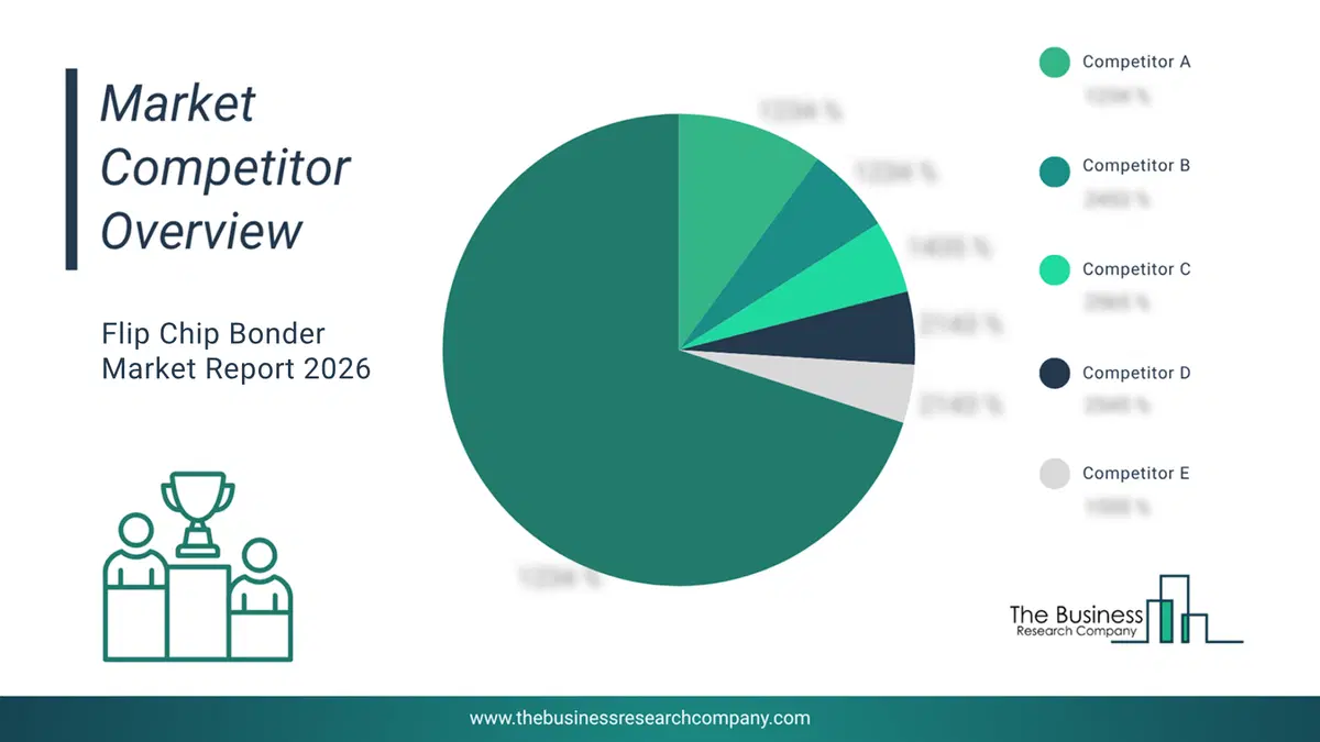
This chart is for illustrative purposes; the full report includes a detailed competitor analysis and comprehensive overview of the top 10 companies in the market.
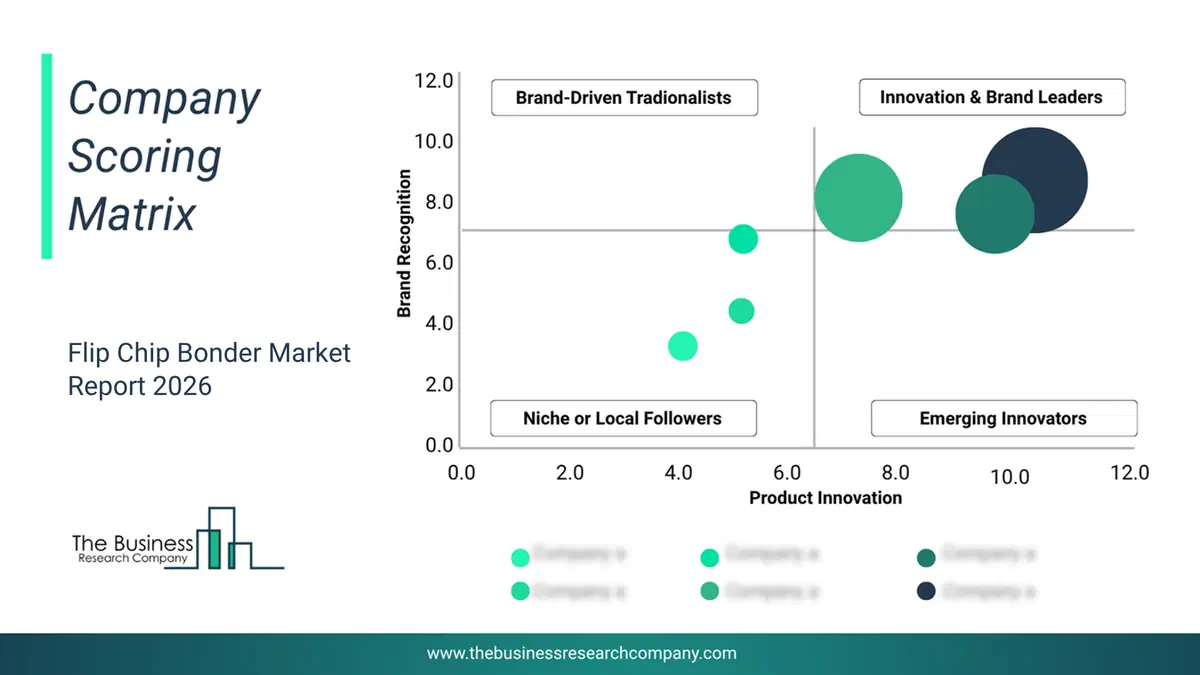
This chart maps companies by product innovation and brand strength, with bubble size indicating relative revenue, helping identify market leaders, challengers, and niche players. This is an illustrative chart; the full report provides a complete and accurate competitive analysis.
Global Flip Chip Bonder Market Trends and Insights
Major companies operating in the flip chip bonder market are focusing on large-die handling capabilities to support advanced semiconductor packaging, accommodate larger chip assemblies, and meet increasing demand from artificial intelligence applications. Large-die handling refers to the ability of bonding equipment to accurately process and assemble substantially larger semiconductor dies and interposer packages while maintaining bonding precision and production stability. For instance, in September 2025, Hanmi Semiconductor, a South Korea-based semiconductor equipment manufacturer, introduced its Big Die FC Bonder, a flip chip bonding solution capable of supporting interposer packages measuring up to 75 mm × 75 mm. The capability is designed to enable the integration of ultra-large dies and multi-chip assemblies used in next-generation AI semiconductors. The equipment supports 2.5D semiconductor packaging, allowing GPUs, CPUs, and high-bandwidth memory (HBM) to be integrated on silicon interposers. The company planned to deploy the equipment on global customers’ mass-production lines, strengthening its capabilities in advanced semiconductor packaging.What Are Latest Mergers And Acquisitions In The Flip Chip Bonder Market?
In April 2025, Applied Materials, Inc., a US-based semiconductor equipment company, acquired a 9% stake in BE Semiconductor Industries N.V. (Besi), for an undisclosed amount. With this acquisition, Applied Materials aims to strengthen its collaboration with Besi in advanced bonding technologies and co-develop an integrated die-to-wafer hybrid bonding system. BE Semiconductor Industries N.V. (Besi) is a Netherlands-based manufacturer of semiconductor assembly equipment, including flip chip bonders and advanced packaging solutions.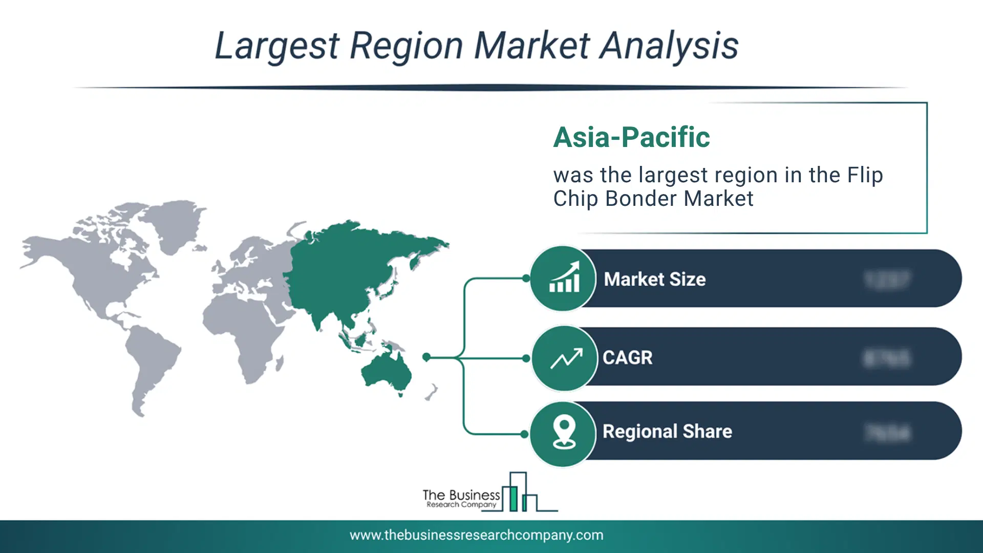
Regional Outlook/Insights
Asia-Pacific was the largest region in the flip chip bonder market in 2025. Asia-Pacific is expected to be the fastest-growing region in the forecast period. The regions covered in this market report are Asia-Pacific, South East Asia, Western Europe, Eastern Europe, North America, South America, Middle East, Africa. The countries covered in this market report are Australia, Brazil, China, France, Germany, India, Indonesia, Japan, Taiwan, Russia, South Korea, UK, USA, Canada, Italy, Spain.What Defines the Flip Chip Bonder Market?
The flip chip bonder market consists of sales of flip chip bonding equipment, wafer-level bonding machines, die placement systems, bump bonding equipment, automated semiconductor assembly equipment, and advanced chip packaging machinery. Values in this market are ‘factory gate’ values, that is, the value of goods sold by the manufacturers or creators of the goods, whether to other entities (including downstream manufacturers, wholesalers, distributors, and retailers) or directly to end customers. The value of goods in this market includes related services sold by the creators of the goods.How is Market Value Defined and Measured?
The market value is defined as the revenues that enterprises gain from the sale of goods and/or services within the specified market and geography through sales, grants, or donations in terms of the currency (in USD unless otherwise specified). The revenues for a specified geography are consumption values that are revenues generated by organizations in the specified geography within the market, irrespective of where they are produced. It does not include revenues from resales along the supply chain, either further along the supply chain or as part of other products.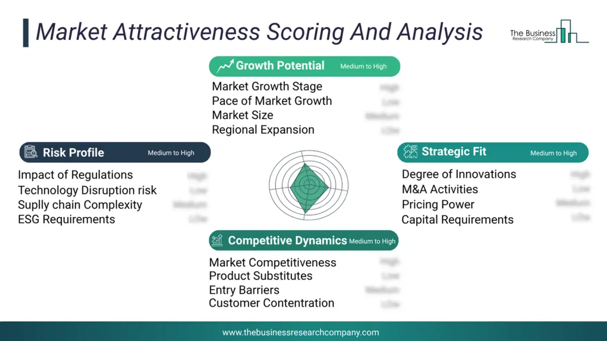
This chart presents market attractiveness based on a quantitative evaluation of growth, competition, strategic alignment, and risk, offering a clear view of opportunity areas for decision-making. This chart is for illustrative purposes; the full report contains the complete analysis.
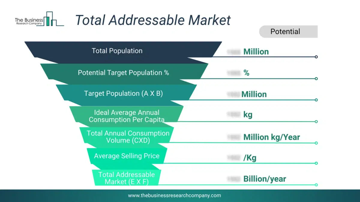
This chart highlights the Total Addressable Market (TAM) by estimating the maximum revenue opportunity using an assumption-driven approach, supporting strategic planning and opportunity sizing across markets. The chart is illustrative; the full report provides a more comprehensive analysis.
What Key Data and Analysis Are Included in the Flip Chip Bonder Market Report 2026?
The flip chip bonder market research report is one of a series of new reports from The Business Research Company that provides market statistics, including industry global market size, regional shares, competitors with the market share, detailed market segments, market trends and opportunities, and any further data you may need to thrive in the flip chip bonder industry. The market research report delivers a complete perspective of everything you need, with an in-depth analysis of the current and future state of the industry.Flip Chip Bonder Market Report Forecast Analysis
| Report Attribute | Details |
|---|---|
| Market Size Value In 2026 | $0.55 billion |
| Revenue Forecast In 2030 | $0.75 billion |
| Growth Rate | CAGR of 8.1% from 2026 to 2035 |
| Base Year For Estimation | 2025 |
| Actual Estimates/Historical Data | 2020-2025 |
| Forecast Period | 2026 - 2030 |
| Market Representation | Revenue in USD Billion and CAGR from 2026 to 2030 |
| Segments Covered | Type, Technology, Packaging Type, Application, End User |
| Regional Scope | Asia-Pacific, Western Europe, Eastern Europe, North America, South America, Middle East, Africa |
| Country Scope | The countries covered in the report are Australia, Brazil, China, France, Germany, India, Indonesia, Japan, Taiwan, Russia, South Korea, UK, USA, Canada, Italy, Spain. |
| Customization Scope | Request for Customization |
| Pricing And Purchase Options | Explore Purchase Options |