

Semiconductor Ceramic Packaging Materials Market Report 2026
Global Outlook – By Type (Alumina Substrates, Aluminum Nitride Substrates, Low Temperature Co Fired Ceramic Substrates), By Packaging Technology (Through Hole Packages, Surface Mount Packages Leaded, Surface Mount Packages Leadless, Advanced Miniaturized Packages, Other Packaging Technologies), By Application (Artificial Intelligence Chip Co Packaged Optics, Heterogeneous Integration, High Thermal Dissipation High Bandwidth Memory), By End Use Industry (Consumer Electronics, Automotive, Healthcare, Information Technology And Telecommunication, Aerospace And Defense) – Market Size, Trends, Strategies, and Forecast to 2035
Semiconductor Ceramic Packaging Materials Market Overview
• Semiconductor Ceramic Packaging Materials market size has reached to $2.74 billion in 2025 • Expected to grow to $4.27 billion in 2030 at a compound annual growth rate (CAGR) of 9.2% • Growth Driver: Increasing Demand For Consumer Electronics Is Fueling The Growth Of The Market Due To Rising Adoption Of Smart Electronic Devices • Market Trend: Advanced Ceramic Substrate Innovations Enhance Semiconductor Packaging Performance And Miniaturization • North America was the largest region in 2025 and Asia-Pacific is the fastest growing region.What Is Covered Under Semiconductor Ceramic Packaging Materials Market?
Semiconductor ceramic packaging materials are ceramic materials used in semiconductor and electronic packaging to provide structural support, electrical insulation, thermal management, and protection for semiconductor devices. Depending on the application, they may offer high mechanical strength, thermal conductivity, dimensional stability, and resistance to harsh operating environments. The main types of semiconductor ceramic packaging materials include alumina substrates, aluminum nitride substrates, and low temperature co fired ceramic substrates. Alumina substrates refer to ceramic materials used as insulating and mechanically stable substrates for semiconductor packaging and electronic circuits. These materials support through hole packages, surface mount packages leaded, surface mount packages leadless, advanced miniaturized packages, and other packaging technologies. The key applications include artificial intelligence chip co packaged optics, heterogeneous integration, and high thermal dissipation high bandwidth memory, while the end-use industries include consumer electronics, automotive, healthcare, information technology and telecommunication, and aerospace and defense industries.
What Is The Semiconductor Ceramic Packaging Materials Market Size and Share 2026?
The semiconductor ceramic packaging materials market size has grown strongly in recent years. It will grow from $2.74 billion in 2025 to $3 billion in 2026 at a compound annual growth rate (CAGR) of 9.6%. The growth in the historic period can be attributed to increasing semiconductor device production, growing adoption of ceramic substrates in power electronics, rising demand for thermal management solutions, expansion of automotive electronics manufacturing, increasing use of ceramic packaging in high-reliability applications.What Is The Semiconductor Ceramic Packaging Materials Market Growth Forecast?
The semiconductor ceramic packaging materials market size is expected to see strong growth in the next few years. It will grow to $4.27 billion in 2030 at a compound annual growth rate (CAGR) of 9.2%. The growth in the forecast period can be attributed to rising demand for high-performance computing chips, increasing adoption of advanced semiconductor packaging technologies, growing demand for high thermal dissipation materials, expansion of heterogeneous integration and chiplet architectures, increasing deployment of high-bandwidth memory applications. Major trends in the forecast period include advanced ceramic substrate materials, high thermal conductivity ceramic packaging, miniaturized ceramic semiconductor packages, multilayer ceramic packaging structures, high-frequency ceramic packaging materials.Tariff Impact On Semiconductor Ceramic Packaging Materials Market
Tariffs are impacting the semiconductor ceramic packaging materials market by increasing the cost of imported ceramic substrates, specialty materials, processing equipment, and semiconductor packaging components. Alumina and aluminum nitride substrates and advanced packaging technologies are likely to face greater cost pressures, particularly across Asia-Pacific, North America, and Europe due to interconnected semiconductor supply chains. However, tariffs may encourage regional sourcing, domestic substrate manufacturing, and supply-chain diversification, while stimulating investment in localized advanced packaging capabilities.

Global Semiconductor Ceramic Packaging Materials Market Segmentation
2) By Packaging Technology: Through Hole Packages, Surface Mount Packages Leaded, Surface Mount Packages Leadless, Advanced Miniaturized Packages, Other Packaging Technologies 3) By Application: Artificial Intelligence Chip Co Packaged Optics, Heterogeneous Integration, High Thermal Dissipation High Bandwidth Memory 4) By End Use Industry: Consumer Electronics, Automotive, Healthcare, Information Technology And Telecommunication, Aerospace And Defense Subsegments: 1) By Alumina Substrates: High Purity Alumina Substrates, Standard Alumina Substrates, Thin Film Alumina Substrates, Thick Film Alumina Substrates 2) By Aluminum Nitride Substrates: High Thermal Conductivity Aluminum Nitride Substrates, Standard Aluminum Nitride Substrates, Direct Bonded Aluminum Nitride Substrates, Metallized Aluminum Nitride Substrates 3) By Low Temperature Co Fired Ceramic Substrates: Glass Ceramic Low Temperature Co Fired Ceramic Substrates, Multilayer Low Temperature Co Fired Ceramic Substrates, Embedded Passive Low Temperature Co Fired Ceramic Substrates, High Frequency Low Temperature Co Fired Ceramic SubstratesWhat Is The Driver Of The Semiconductor Ceramic Packaging Materials Market?
The growing expansion of consumer electronics manufacturing is expected to propel the growth of the semiconductor ceramic packaging materials market going forward. Consumer electronics are electronic devices such as smartphones, laptops, tablets, wearables, televisions, and smart home products used by individuals for communication, entertainment, productivity, and everyday activities. Consumer electronics demand is increasing due to rising consumer spending on smart devices, driven by the need for better connectivity, productivity, and entertainment. The growing expansion of consumer electronics manufacturing increases the need for semiconductor ceramic packaging materials as advanced electronic devices require highly reliable ceramic substrates and packages that provide efficient heat dissipation, electrical insulation, and long-term performance in compact designs. May 2025, according to the Japan Electronics and Information Technology Industries Association (JEITA), a Japan-based trade association, consumer electronic equipment production in Japan reached $221.5 million (¥31.9 billion) in May 2025, representing 103.3% of the level recorded in May 2024, or a 3.3% year-over-year increase. Therefore, the growing expansion of consumer electronics manufacturing is driving the growth of the semiconductor ceramic packaging materials industry.Key Players In The Global Semiconductor Ceramic Packaging Materials Market
Major companies operating in the semiconductor ceramic packaging materials market are Resonac Holdings Corporation, Kyocera Corporation, CeramTec GmbH, Niterra Co. Ltd., TOTO Advanced Ceramics Co. Ltd., NGK Insulators Ltd., Denka Company Limited, Tokuyama Corporation, Materion Corporation, CoorsTek Inc., Ferrotec Holdings Corporation, Morgan Advanced Materials plc, Chaozhou Three-Circle Group Co. Ltd., Maruwa Co. Ltd., St.Cera Co. Ltd., INNOVACERA Advanced Materials Co. Ltd., Leatec Fine Ceramics Co. Ltd., ASUZAC Fine Ceramics Co. Ltd., AGC Inc., Shanghai Companion Precision Ceramics Co. Ltd., Nishimura Advanced Ceramics Co. Ltd., Advanced Ceramic X Corp., Orbray Co. Ltd., Precision Ferrites and Ceramics Pvt. Ltd.
This chart is for illustrative purposes; the full report includes a detailed competitor analysis and comprehensive overview of the top 10 companies in the market.

This chart maps companies by product innovation and brand strength, with bubble size indicating relative revenue, helping identify market leaders, challengers, and niche players. This is an illustrative chart; the full report provides a complete and accurate competitive analysis.
Global Semiconductor Ceramic Packaging Materials Market Trends and Insights
Major companies operating in the semiconductor ceramic packaging materials market are focusing on developing advanced ceramic substrate solutions to enhance packaging rigidity, reduce warpage, enable high-density wiring, and support the miniaturization of advanced semiconductor packages. Ceramic substrate solutions are advanced ceramic-based materials used in semiconductor packages to provide electrical insulation, mechanical stability, and efficient heat dissipation while supporting high-density wiring and device miniaturization. For instance, in April 2026, Kyocera Corporation, a Japan-based manufacturer of advanced ceramic and electronic components, announced the commercialization of a new multilayer ceramic core substrate for advanced semiconductor packages, including xPUs and switch ASICs. Built using proprietary fine ceramic materials, the substrate provides exceptional rigidity to minimize warpage while enabling finer wiring and circuit miniaturization, supporting the evolving packaging requirements of AI data centers and high-performance semiconductors.What Are Latest Mergers And Acquisitions In The Semiconductor Ceramic Packaging Materials Market?
In February 2026, Element Solutions Inc., a US-based specialty chemicals and electronic materials company, acquired Micromax conductive pastes and inks business for an undisclosed amount. With this acquisition, Element Solutions Inc. aims to strengthen its position as a global supplier of specialized electronic materials, expand its portfolio of conductive pastes, inks, and ceramic materials, enhance its capabilities for advanced and high-reliability electronics applications, broaden its solutions for automotive and advanced mobility, telecommunications/5G, consumer electronics, aerospace and defense, and medical devices, and support customers with improved performance, reliability, and design flexibility. Micromax is a US-based electronic materials business that specializes in providing semiconductor ceramic packaging materials.
Regional Outlook/Insights
North America was the largest region in the semiconductor ceramic packaging materials market in 2025. Asia-Pacific is expected to be the fastest-growing region in the forecast period. The regions covered in this market report are Asia-Pacific, South East Asia, Western Europe, Eastern Europe, North America, South America, Middle East, Africa. The countries covered in this market report are Australia, Brazil, China, France, Germany, India, Indonesia, Japan, Taiwan, Russia, South Korea, UK, USA, Canada, Italy, Spain.What Defines the Semiconductor Ceramic Packaging Materials Market?
The semiconductor ceramic packaging materials market consists of sales of beryllium oxide ceramic substrates, ceramic package bodies, ceramic encapsulation materials, ceramic heat spreader materials, and other advanced ceramic packaging materials. Values in this market are ‘factory gate’ values, that is, the value of goods sold by manufacturers or creators of the goods, whether to other entities (including downstream manufacturers, wholesalers, distributors, and retailers) or directly to end customers. The value of goods in this market includes related services sold by the creators of the goods.How is Market Value Defined and Measured?
The market value is defined as the revenues that enterprises gain from the sale of goods and/or services within the specified market and geography through sales, grants, or donations in terms of the currency (in USD unless otherwise specified). The revenues for a specified geography are consumption values that are revenues generated by organizations in the specified geography within the market, irrespective of where they are produced. It does not include revenues from resales along the supply chain, either further along the supply chain or as part of other products.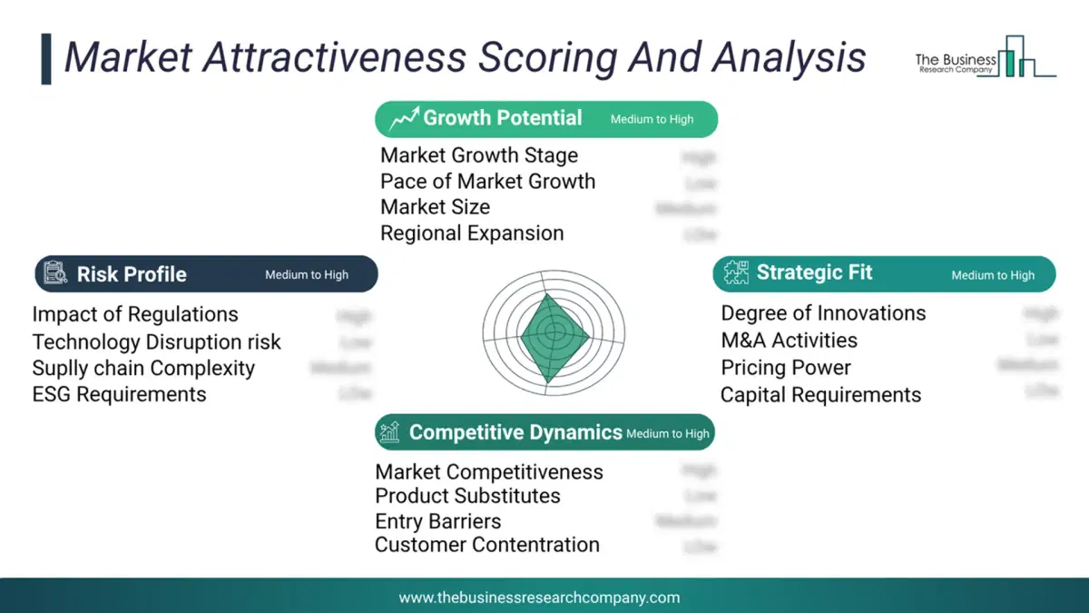
This chart presents market attractiveness based on a quantitative evaluation of growth, competition, strategic alignment, and risk, offering a clear view of opportunity areas for decision-making. This chart is for illustrative purposes; the full report contains the complete analysis.
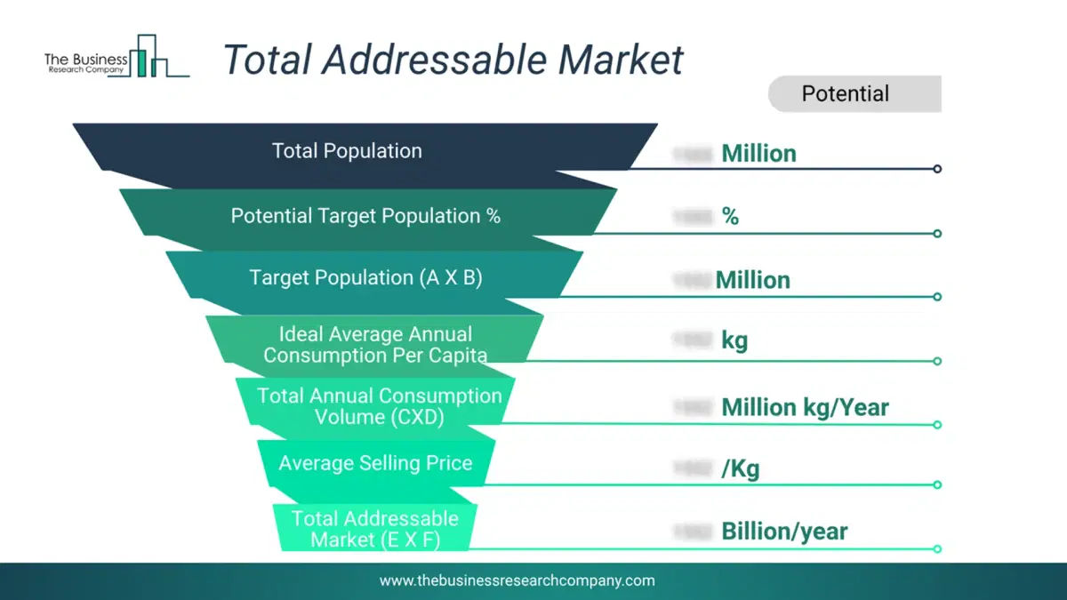
This chart highlights the Total Addressable Market (TAM) by estimating the maximum revenue opportunity using an assumption-driven approach, supporting strategic planning and opportunity sizing across markets. The chart is illustrative; the full report provides a more comprehensive analysis.
What Key Data and Analysis Are Included in the Semiconductor Ceramic Packaging Materials Market Report 2026?
The semiconductor ceramic packaging materials market research report is one of a series of new reports from The Business Research Company that provides market statistics, including industry global market size, regional shares, competitors with the market share, detailed market segments, market trends and opportunities, and any further data you may need to thrive in the semiconductor ceramic packaging materials industry. The market research report delivers a complete perspective of everything you need, with an in-depth analysis of the current and future state of the industry.Semiconductor Ceramic Packaging Materials Market Report Forecast Analysis
| Report Attribute | Details |
|---|---|
| Market Size Value In 2026 | $3 billion |
| Revenue Forecast In 2030 | $4.27 billion |
| Growth Rate | CAGR of 9.2% from 2026 to 2035 |
| Base Year For Estimation | 2025 |
| Actual Estimates/Historical Data | 2020-2025 |
| Forecast Period | 2026 - 2030 |
| Market Representation | Revenue in USD Billion and CAGR from 2026 to 2030 |
| Segments Covered | Type, Packaging Technology, Application, End Use Industry |
| Regional Scope | Asia-Pacific, Western Europe, Eastern Europe, North America, South America, Middle East, Africa |
| Country Scope | The countries covered in the report are Australia, Brazil, China, France, Germany, India, Indonesia, Japan, Taiwan, Russia, South Korea, UK, USA, Canada, Italy, Spain. |
| Customization Scope | Request for Customization |
| Pricing And Purchase Options | Explore Purchase Options |