

Semiconductor Inspection and Measurement Equipment Market Report 2026
Global Outlook – By Equipment Type (Wafer Inspection Equipment, Mask Inspection Equipment, Metrology Equipment, Defect Review Equipment, Thin Film Measurement Equipment, Other Equipment Types), By Technology (Optical Inspection, Scanned Probe Microscopy, Electron Beam Inspection, X-Ray Inspection, Infrared Inspection), By Automation Level (Fully Automated Equipment, Semi-Automated Equipment, Manual Equipment), By End User (Semiconductor Foundries, Integrated Device Manufacturers, Research Institutions, Electronics Manufacturers, Aerospace And Defense Sector) – Market Size, Trends, Strategies, and Forecast to 2035
Semiconductor Inspection and Measurement Equipment Market Overview
• Semiconductor Inspection and Measurement Equipment market size has reached to $13.62 billion in 2025 • Expected to grow to $19.5 billion in 2030 at a compound annual growth rate (CAGR) of 7.3% • Growth Driver: Rising Adoption Of Advanced Packaging Technologies Fueling The Growth Of The Market Due To Increasing Demand For High-Performance Semiconductor Devices • Market Trend: Innovations In Inspection And Metrology Technologies Enhance Semiconductor Defect Detection And Process Control • Asia-Pacific was the largest region and fastest growing region.What Is Covered Under Semiconductor Inspection and Measurement Equipment Market?
Semiconductor inspection and measurement equipment refers to specialized machines used to inspect, measure, and analyze semiconductor wafers, chips, and related components during the manufacturing process to ensure they meet precise design and quality requirements. These systems use advanced optical, electron beam, X-ray, and metrology technologies to detect defects, verify dimensions, and monitor process accuracy at various production stages. They play a vital role in improving manufacturing precision, increasing production yield, and supporting the fabrication of advanced semiconductor devices. The main equipment types of semiconductor inspection and measurement equipment include wafer inspection equipment, mask inspection equipment, metrology equipment, defect review equipment, thin film measurement equipment, and other equipment types. Wafer inspection equipment refers to specialized systems used to examine semiconductor wafers for defects, irregularities, and process variations to help ensure manufacturing quality and consistency. These systems use optical inspection, scanned probe microscopy, electron beam inspection, X-ray inspection, and infrared inspection technologies. They are available as fully automated equipment, semi-automated equipment, and manual equipment, and are used end users by semiconductor foundries, integrated device manufacturers, research institutions, electronics manufacturers, and the aerospace and defense sector.
What Is The Semiconductor Inspection and Measurement Equipment Market Size and Share 2026?
The semiconductor inspection and measurement equipment market size has grown strongly in recent years. It will grow from $13.62 billion in 2025 to $14.68 billion in 2026 at a compound annual growth rate (CAGR) of 7.8%. The growth in the historic period can be attributed to increasing semiconductor manufacturing capacity, rising demand for defect detection and yield improvement, growing adoption of advanced semiconductor nodes, increasing complexity of semiconductor device architectures, expansion of wafer-level process monitoring.What Is The Semiconductor Inspection and Measurement Equipment Market Growth Forecast?
The semiconductor inspection and measurement equipment market size is expected to see strong growth in the next few years. It will grow to $19.5 billion in 2030 at a compound annual growth rate (CAGR) of 7.3%. The growth in the forecast period can be attributed to increasing production of advanced logic and memory devices, rising demand for high-resolution metrology, growing adoption of heterogeneous integration and advanced packaging, increasing need for real-time process control, expansion of semiconductor fabrication investments. Major trends in the forecast period include AI-enabled defect detection, advanced semiconductor process control, high-precision nanoscale metrology, hybrid optical and electron beam inspection, in-line wafer quality monitoring.Tariff Impact On Semiconductor Inspection and Measurement Equipment Market
Tariffs are impacting the semiconductor inspection and measurement equipment market by increasing the cost of imported inspection systems, precision components, optical modules, sensors, and specialized manufacturing equipment. Wafer inspection, metrology, and defect review equipment segments are likely to face greater cost pressures, particularly in Asia-Pacific, North America, and Europe due to globally interconnected semiconductor equipment supply chains. Higher equipment costs may delay capacity expansions and equipment upgrades, while tariffs can also encourage localized manufacturing, supplier diversification, and regional semiconductor equipment production, creating opportunities for domestic suppliers.

Global Semiconductor Inspection and Measurement Equipment Market Segmentation
2) By Technology: Optical Inspection, Scanned Probe Microscopy, Electron Beam Inspection, X-Ray Inspection, Infrared Inspection 3) By Automation Level: Fully Automated Equipment, Semi-Automated Equipment, Manual Equipment 4) By End User: Semiconductor Foundries, Integrated Device Manufacturers, Research Institutions, Electronics Manufacturers, Aerospace And Defense Sector Subsegments: 1) By Wafer Inspection Equipment: Bright Field Wafer Inspection Equipment, Dark Field Wafer Inspection Equipment, Surface Inspection Equipment, Edge Inspection Equipment, Patterned Wafer Inspection Equipment 2) By Mask Inspection Equipment: Reticle Inspection Equipment, Photomask Defect Inspection Equipment, Pattern Inspection Equipment, Particle Inspection Equipment, Critical Dimension Mask Inspection Equipment 3) By Metrology Equipment: Critical Dimension Measurement Equipment, Overlay Measurement Equipment, Thickness Measurement Equipment, Surface Profile Measurement Equipment, Optical Measurement Equipment 4) By Defect Review Equipment: Electron Beam Defect Review Equipment, Optical Defect Review Equipment, Automated Defect Classification Equipment, High Resolution Defect Review Equipment, Three Dimensional Defect Review Equipment 5) By Thin Film Measurement Equipment: Film Thickness Measurement Equipment, Refractive Index Measurement Equipment, Stress Measurement Equipment, Surface Roughness Measurement Equipment, Optical Film Characterization Equipment 6) By Other Equipment Types: Contamination Inspection Equipment, Package Inspection Equipment, Bond Inspection Equipment, Material Characterization Equipment, Hybrid Inspection EquipmentWhat Is The Driver Of The Semiconductor Inspection and Measurement Equipment Market?
The rising adoption of advanced packaging technologies is expected to propel the growth of the semiconductor inspection and measurement equipment market going forward. Advanced packaging technologies are semiconductor packaging methods that integrate multiple chips or components into a single package using techniques such as chiplets, 2.5D packaging, 3D stacking, and heterogeneous integration to enhance device performance, power efficiency, and functionality. Advanced packaging technologies are increasing due to the growing demand for artificial intelligence (AI) applications, which require higher computing performance and greater chip integration. Semiconductor inspection and measurement equipment supports advanced packaging technologies by enabling precise defect detection, dimensional measurement, alignment verification, and process control throughout the packaging process. For instance, in July 2026, according to the National Institute of Standards and Technology (NIST), a US-based government agency, the CHIPS for America program announced up to $490 million in federal incentives for advanced-packaging-related semiconductor R&D, including up to $300 million for GlobalFoundries, $140 million for Multibeam Corporation, and $50 million for Thintronics, highlighting growing support for the expansion and adoption of advanced semiconductor packaging technologies. Therefore, the rising adoption of advanced packaging technologies is driving the growth of the semiconductor inspection and measurement equipment industry.Key Players In The Global Semiconductor Inspection and Measurement Equipment Market
Major companies operating in the semiconductor inspection and measurement equipment market are Applied Materials Inc., ASML Holding N.V., KLA Corporation, Lasertec Corporation, Carl Zeiss SMT GmbH, Lam Research Corporation, Advantest Corporation, Tokyo Electron Limited, Hitachi High-Tech Corporation, Onto Innovation Inc., Nova Ltd., Camtek Ltd., Thermo Fisher Scientific Inc., JEOL Ltd., FormFactor Inc., Tokyo Seimitsu Co. Ltd., Veeco Instruments Inc., Park Systems Corp., Rigaku Holdings Corporation, Nikon Corporation, Keysight Technologies Inc., HORIBA Ltd., Bruker Corporation, SENTECH Instruments GmbH, Sensofar Tech S.L.
This chart is for illustrative purposes; the full report includes a detailed competitor analysis and comprehensive overview of the top 10 companies in the market.

This chart maps companies by product innovation and brand strength, with bubble size indicating relative revenue, helping identify market leaders, challengers, and niche players. This is an illustrative chart; the full report provides a complete and accurate competitive analysis.
Global Semiconductor Inspection and Measurement Equipment Market Trends and Insights
Major companies operating in the semiconductor inspection and measurement equipment market are focusing on developing advanced solutions, such as high-sensitivity inspection and metrology platforms, to improve defect detection, measurement accuracy, throughput, and process control across advanced semiconductor manufacturing. High-sensitivity inspection and metrology platforms refer to equipment that combines high-resolution imaging, defect detection, and dimensional measurement technologies to identify submicron defects and support precise semiconductor process control. For instance, in March 2026, Onto Innovation Inc., a US-based semiconductor process control equipment company, launched the Dragonfly G5 system, a new inspection and metrology platform designed for front-end and advanced packaging applications. The system combines 150 nm defect sensitivity, brightfield and darkfield inspection, and machine-learning algorithms for enhanced defect detection. It also provides 3D metrology and sub-surface inspection, helping improve yield and process control in advanced packaging and high-bandwidth memory applications.What Are Latest Mergers And Acquisitions In The Semiconductor Inspection and Measurement Equipment Market?
In February 2025, Nova Ltd., an Israel-based provider of metrology and process control solutions for semiconductor manufacturing, completed the acquisition of Sentronics Metrology GmbH for approximately $60 million. Through this acquisition, Nova aims to expand its semiconductor inspection and measurement capabilities by integrating Sentronics’ modular wafer metrology technologies into its dimensional metrology portfolio, particularly for advanced wafer-level packaging and specialty devices. Sentronics Metrology GmbH is a Germany-based provider of wafer metrology tools for backend semiconductor fabrication, offering metrology systems for measuring critical parameters such as thickness, roughness, and topography.
Regional Outlook/Insights
Asia-Pacific was the largest region in the semiconductor inspection and measurement equipment market in 2025. Asia-Pacific is expected to be the fastest-growing region in the forecast period. The regions covered in this market report are Asia-Pacific, South East Asia, Western Europe, Eastern Europe, North America, South America, Middle East, Africa. The countries covered in this market report are Australia, Brazil, China, France, Germany, India, Indonesia, Japan, Taiwan, Russia, South Korea, UK, USA, Canada, Italy, Spain.What Defines the Semiconductor Inspection and Measurement Equipment Market?
The semiconductor inspection and measurement equipment market consists of sales of inspection systems, optical inspection systems, electron beam inspection systems, overlay measurement systems, and critical dimension measurement systems. Values in this market are ‘factory gate’ values, that is the value of goods sold by the manufacturers or creators of the goods, whether to other entities (including downstream manufacturers, wholesalers, distributors and retailers) or directly to end customers. The value of goods in this market includes related services sold by the creators of the goods.How is Market Value Defined and Measured?
The market value is defined as the revenues that enterprises gain from the sale of goods and/or services within the specified market and geography through sales, grants, or donations in terms of the currency (in USD unless otherwise specified). The revenues for a specified geography are consumption values that are revenues generated by organizations in the specified geography within the market, irrespective of where they are produced. It does not include revenues from resales along the supply chain, either further along the supply chain or as part of other products.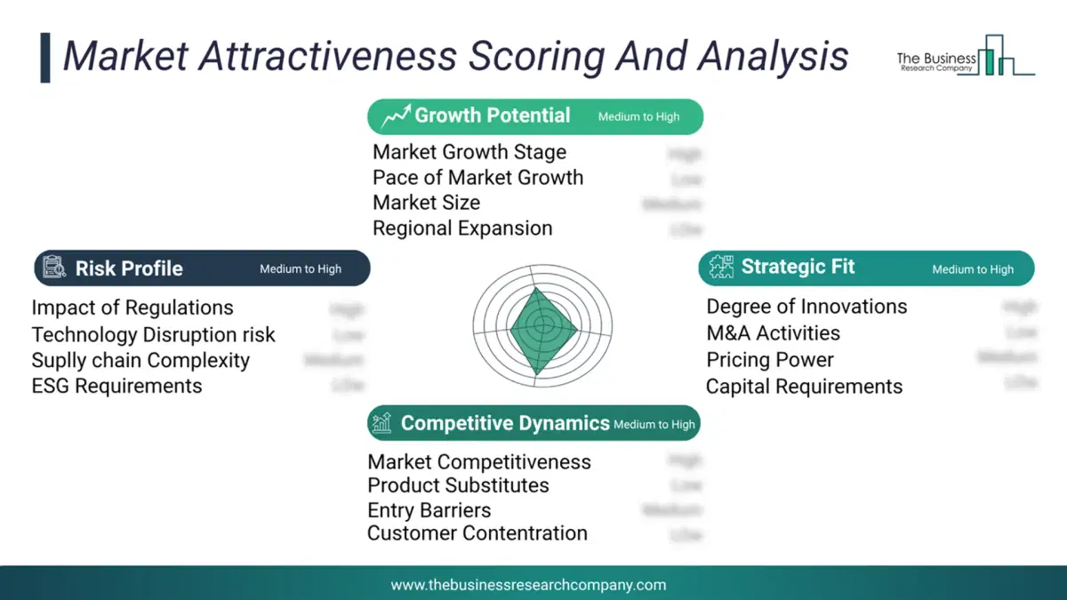
This chart presents market attractiveness based on a quantitative evaluation of growth, competition, strategic alignment, and risk, offering a clear view of opportunity areas for decision-making. This chart is for illustrative purposes; the full report contains the complete analysis.
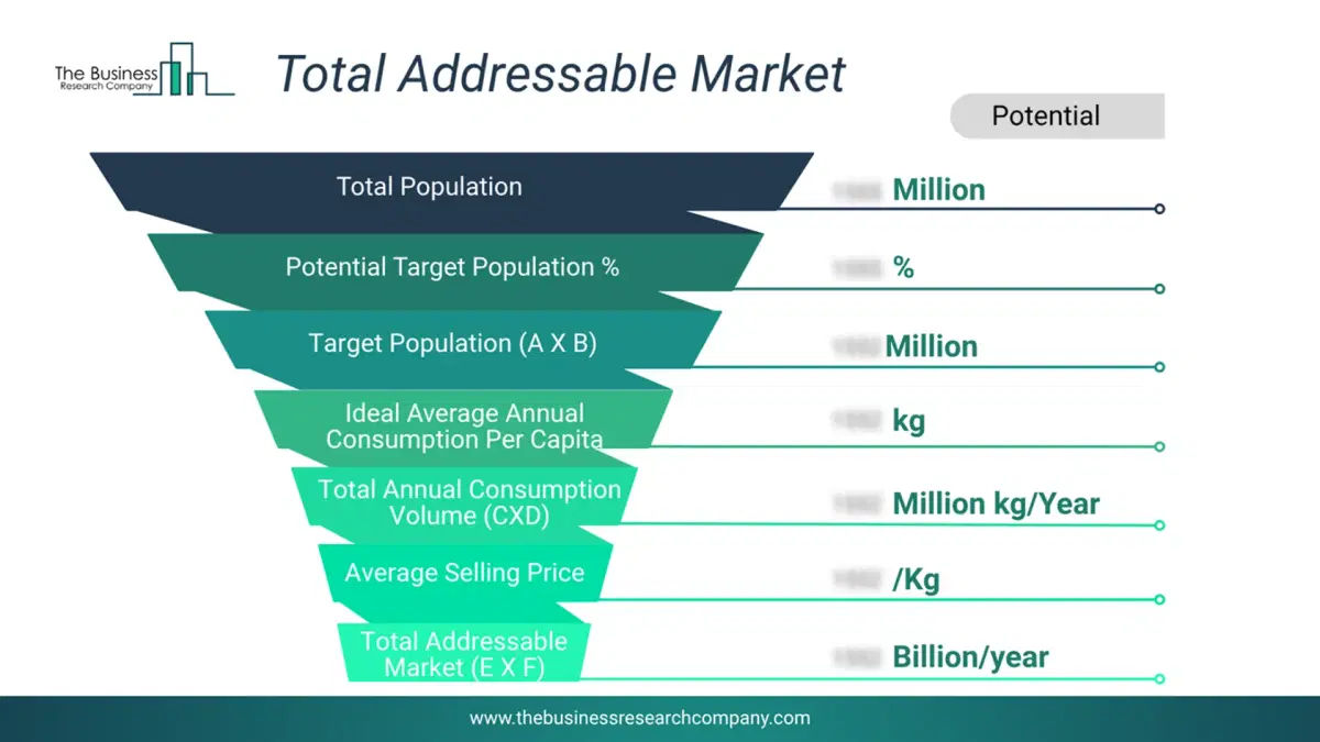
This chart highlights the Total Addressable Market (TAM) by estimating the maximum revenue opportunity using an assumption-driven approach, supporting strategic planning and opportunity sizing across markets. The chart is illustrative; the full report provides a more comprehensive analysis.
What Key Data and Analysis Are Included in the Semiconductor Inspection and Measurement Equipment Market Report 2026?
The semiconductor inspection and measurement equipment market research report is one of a series of new reports from The Business Research Company that provides market statistics, including industry global market size, regional shares, competitors with the market share, detailed market segments, market trends and opportunities, and any further data you may need to thrive in the semiconductor inspection and measurement equipment industry. The market research report delivers a complete perspective of everything you need, with an in-depth analysis of the current and future state of the industry.Semiconductor Inspection and Measurement Equipment Market Report Forecast Analysis
| Report Attribute | Details |
|---|---|
| Market Size Value In 2026 | $14.68 billion |
| Revenue Forecast In 2030 | $19.5 billion |
| Growth Rate | CAGR of 7.3% from 2026 to 2035 |
| Base Year For Estimation | 2025 |
| Actual Estimates/Historical Data | 2020-2025 |
| Forecast Period | 2026 - 2030 |
| Market Representation | Revenue in USD Billion and CAGR from 2026 to 2030 |
| Segments Covered | Equipment Type, Technology, Automation Level, End User |
| Regional Scope | Asia-Pacific, Western Europe, Eastern Europe, North America, South America, Middle East, Africa |
| Country Scope | The countries covered in the report are Australia, Brazil, China, France, Germany, India, Indonesia, Japan, Taiwan, Russia, South Korea, UK, USA, Canada, Italy, Spain. |
| Customization Scope | Request for Customization |
| Pricing And Purchase Options | Explore Purchase Options |