
Semiconductor Packaging Market Report 2026
Global Outlook – By Packaging Type (Dual In-Line Package, Quad Flat Package, Ball Grid Array, Chip Scale Package, System In Package, Wafer Level Packaging), By Material (Organic Substrate, Bonding Wire, Leadframes, Encapsulation Resins, Ceramic Package, Die Attach Material, Thermal Interface Materials, Solder Balls, Others (e)g), Adhesives, Underfill, Specialty Films)), By Technology (Advanced Packaging, Flip Chip, System In Package (SiP), By Application (Analog And Mixed Signal, Wireless Connectivity, Optoelectronic, Micro Electro Mechanical Systems And Sensor, Miscellaneous Logic And Memory), By End-Use (Consumer Electronics, Automotive, Healthcare, Information Technology And Telecommunication, Aerospace And Defence) – Market Size, Trends, Strategies, and Forecast to 2030
Semiconductor Packaging Market Overview
• Semiconductor Packaging market size has reached to $39.55 billion in 2025 • Expected to grow to $60.64 billion in 2030 at a compound annual growth rate (CAGR) of 9% • Growth Driver: Growing Demand For Consumer Electronics Driving The Market Growth Due To Rising Smartphone And Internet Penetration • Market Trend: Leading Companies Driving Technological Advancements In High-Performance Chip Integration • Asia-Pacific was the largest region in 2025 and North America is the fastest growing region.What Is Covered Under Semiconductor Packaging Market?
Semiconductor packaging refers to the process of enclosing and protecting a semiconductor chip after fabrication, providing mechanical support, electrical connections, and thermal management to ensure reliable operation in electronic devices. Its applications span consumer electronics, computing systems, telecommunications equipment, automotive technologies, medical devices, and industrial electronics, where packaged semiconductor components play a critical role in processing, memory storage, sensing, and power management. The main types of semiconductor packaging include dual in-line package, quad flat package, ball grid array, chip scale package, system in package, and wafer level packaging. Dual in-line package refers to a through-hole packaging format with two parallel rows of pins used for mounting integrated circuits onto printed circuit boards. These are manufactured using materials such as organic substrate, bonding wire, leadframes, encapsulation resins, ceramic package, die attach material, thermal interface materials, solder balls, and others including adhesives, underfill, and specialty films and are enabled by technologies including advanced packaging, flip chip, system in package (SiP), 2.5D or 3D packaging, embedded die, fan-in wafer level packaging (FI-WLP), fan-out wafer level packaging (FO-WLP), and others for various applications including analog and mixed signal, wireless connectivity, optoelectronic, micro electro mechanical systems and sensor, and miscellaneous logic and memory. The main end-uses include consumer electronics, automotive, healthcare, information technology and telecommunication, and aerospace and defence.
What Is The Semiconductor Packaging Market Size and Share 2026?
The semiconductor packaging market size has grown strongly in recent years. It will grow from $39.55 billion in 2025 to $43.01 billion in 2026 at a compound annual growth rate (CAGR) of 8.7%. The growth in the historic period can be attributed to increasing demand for consumer electronics, growth of semiconductor manufacturing, rising need for miniaturized devices, adoption of flip-chip and advanced packaging methods, expansion of automotive electronics.What Is The Semiconductor Packaging Market Growth Forecast?
The semiconductor packaging market size is expected to see strong growth in the next few years. It will grow to $60.64 billion in 2030 at a compound annual growth rate (CAGR) of 9.0%. The growth in the forecast period can be attributed to growing adoption of ai-enabled semiconductor devices, rising demand for 5g and wireless connectivity chips, expansion of automotive electrification, increasing deployment of iot devices, growing requirement for high-performance computing and memory chips. Major trends in the forecast period include rising adoption of Advanced Packaging Technologies, growing demand for fan-out and 3d packaging solutions, increasing integration of thermal management materials, expansion of testing and quality assurance services, rising focus on miniaturization and high-density packaging.

Global Semiconductor Packaging Market Segmentation
1) By Packaging Type: Dual In-Line Package, Quad Flat Package, Ball Grid Array, Chip Scale Package, System In Package, Wafer Level Packaging 2) By Material: Organic Substrate, Bonding Wire, Leadframes, Encapsulation Resins, Ceramic Package, Die Attach Material, Thermal Interface Materials, Solder Balls, Others (e)g), Adhesives, Underfill, Specialty Films) 3) By Technology: Advanced Packaging, Flip Chip, System In Package (SiP), 2)5D Or 3D Packaging, Embedded Die, Fan-In Wafer Level Packaging (FI-WLP), Fan-Out Wafer Level Packaging (FO-WLP), Other Technologies 4) By Application: Analog And Mixed Signal, Wireless Connectivity, Optoelectronic, Micro Electro Mechanical Systems And Sensor, Miscellaneous Logic And Memory 5) By End-Use: Consumer Electronics, Automotive, Healthcare, Information Technology And Telecommunication, Aerospace And Defence Subsegments: 1) By Dual In-Line Package: Through Hole Mount, Surface Mount, Single Row Lead, Multiple Row Lead, High Pin Count, Low Pin Count 2) By Quad Flat Package: Standard Quad Flat Package, Thin Quad Flat Package, Leadless Quad Flat Package, Plastic Quad Flat Package, Ceramic Quad Flat Package, Low Profile Quad Flat Package 3) By Ball Grid Array: Fine Pitch Ball Grid Array, Column Grid Array, Micro Ball Grid Array, Plastic Ball Grid Array, Ceramic Ball Grid Array, High Density Ball Grid Array 4) By Chip Scale Package: Standard Chip Scale Package, Wafer Level Chip Scale Package, Fan In Chip Scale Package, Fan Out Chip Scale Package, Embedded Chip Scale Package, Low Profile Chip Scale Package 5) By System In Package: Multi Chip Module, Stacked Die System In Package, Package On Package, Embedded Die System In Package, Fan In System In Package, Fan Out System In Package 6) By Wafer Level Packaging: Fan In Wafer Level Packaging, Fan Out Wafer Level Packaging, Redistribution Layer Wafer Level Packaging, Embedded Wafer Level Packaging, Through Silicon Via Wafer Level Packaging, Panel Level Wafer Level PackagingWhat Is The Driver Of The Semiconductor Packaging Market?
The growing demand for consumer electronics is expected to propel the growth of the semiconductor packaging market going forward. Consumer electronics refers to electronic devices made for personal or home use that provide entertainment, communication, or practical functionality. The demand for consumer electronics is increasing due to rising smartphone and internet penetration, which drives the adoption of connected devices for communication, entertainment, and smart living. Semiconductor packaging ensures the performance and durability of consumer electronics by safeguarding chips, managing heat, and facilitating efficient electrical connectivity. For instance, in May 2023, according to the Japan Electronics and Information Technology Industries Association, a Japan-based trade association, consumer electronics output increasing from $183 million in May 2022 to $233 million in May 2023. Therefore, the growing demand for consumer electronics is driving the growth of the semiconductor packaging industry.Key Players In The Global Semiconductor Packaging Market
Major companies operating in the semiconductor packaging market are Samsung Electronics Co. Ltd., Taiwan Semiconductor Manufacturing Company Ltd., Intel Corporation, ASE Technology Holding Co. Ltd., Amkor Technology Inc., JCET Group Co. Ltd., Siliconware Precision Industries Co. Ltd., Powertech Technology Inc., STATS ChipPAC Pte. Ltd., Tianshui Huatian Technology Co. Ltd., King Yuan Electronics Co. Ltd., UTAC Holdings Ltd., ChipMOS Technologies Inc., OSE Co. Ltd., Hana Micron Inc., Unisem (M) Berhad, Nepes Corporation, Formosa Advanced Technologies Co. Ltd., Walton Advanced Engineering Inc., AOI Electronics Co. Ltd., China Wafer Level CSP Co. Ltd., Tongfu Microelectronics Co. Ltd., Chipbond Technology Corporation, and Cactus Materials Inc.
This chart is for illustrative purposes; the full report includes a detailed competitor analysis and comprehensive overview of the top 10 companies in the market.

This chart maps companies by product innovation and brand strength, with bubble size indicating relative revenue, helping identify market leaders, challengers, and niche players. This is an illustrative chart; the full report provides a complete and accurate competitive analysis.
Global Semiconductor Packaging Market Trends and Insights
Major companies operating in the semiconductor packaging market are focusing on technological advancements such as, panel-level organic interposers to enhance interconnect density, improve thermal performance, and enable cost-effective high-performance packaging for advanced semiconductor devices. A panel-level organic interposer refers to a large organic substrate that connects multiple chips on a single panel, allowing high-density interconnections at lower cost compared to wafer-level approaches. These interposers are particularly attractive for AI and high-performance computing applications due to their scalability and improved manufacturing efficiency. For instance, in September 2025, Resonac Corp., a Japan-based chemical manufacturing company, announced the formation of the JOINT3 consortium to develop next-generation semiconductor packaging solutions. The initiative focuses on developing panel-level organic interposers (515 × 510 mm prototypes) to address growing AI and HPC demand, with prototype operations planned for 2026. Led by Resonac through its Advanced Panel Level Interposer Center in Japan, JOINT3 aims to promote co-creation across materials, equipment, and design tools for advanced 2.5D packaging.What Are Latest Mergers And Acquisitions In The Semiconductor Packaging Market?
In December 2025, ROHM Co. Ltd., a Japan-based manufacturing company, partnered with Tata Electronics Private Limited to expand semiconductor component supply and enhance joint research in advanced electronic devices. With this partnership, companies aim to establish power semiconductor manufacturing in India through ROHM's design-process technology integration and Tata's backend packaging assembly for automotive and global markets. Tata Electronics Private Limited is an India-based electronics manufacturing company that offers semiconductor packaging solutions.
Regional Insights
Asia-Pacific was the largest region in the semiconductor packaging market in 2025. North America is expected to be the fastest-growing region in the forecast period. The regions covered in this market report are Asia-Pacific, South East Asia, Western Europe, Eastern Europe, North America, South America, Middle East, Africa. The countries covered in this market report are Australia, Brazil, China, France, Germany, India, Indonesia, Japan, Taiwan, Russia, South Korea, UK, USA, Canada, Italy, Spain.What Defines the Semiconductor Packaging Market?
The semiconductor packaging market consists of revenues earned by entities by providing services such as chip encapsulation, thermal management, and testing and quality assurance. The market value includes the value of related goods sold by the service provider or included within the service offering. The semiconductor packaging market also includes sales of plastic leaded chip carriers, ceramic leadless chip carriers, and wafer-level packages. Values in this market are ‘factory gate’ values; that is, the value of goods sold by the manufacturers or creators of the goods, whether to other entities (including downstream manufacturers, wholesalers, distributors, and retailers) or directly to end customers. The value of goods in this market includes related services sold by the creators of the goods.How is Market Value Defined and Measured?
The market value is defined as the revenues that enterprises gain from the sale of goods and/or services within the specified market and geography through sales, grants, or donations in terms of the currency (in USD unless otherwise specified). The revenues for a specified geography are consumption values that are revenues generated by organizations in the specified geography within the market, irrespective of where they are produced. It does not include revenues from resales along the supply chain, either further along the supply chain or as part of other products.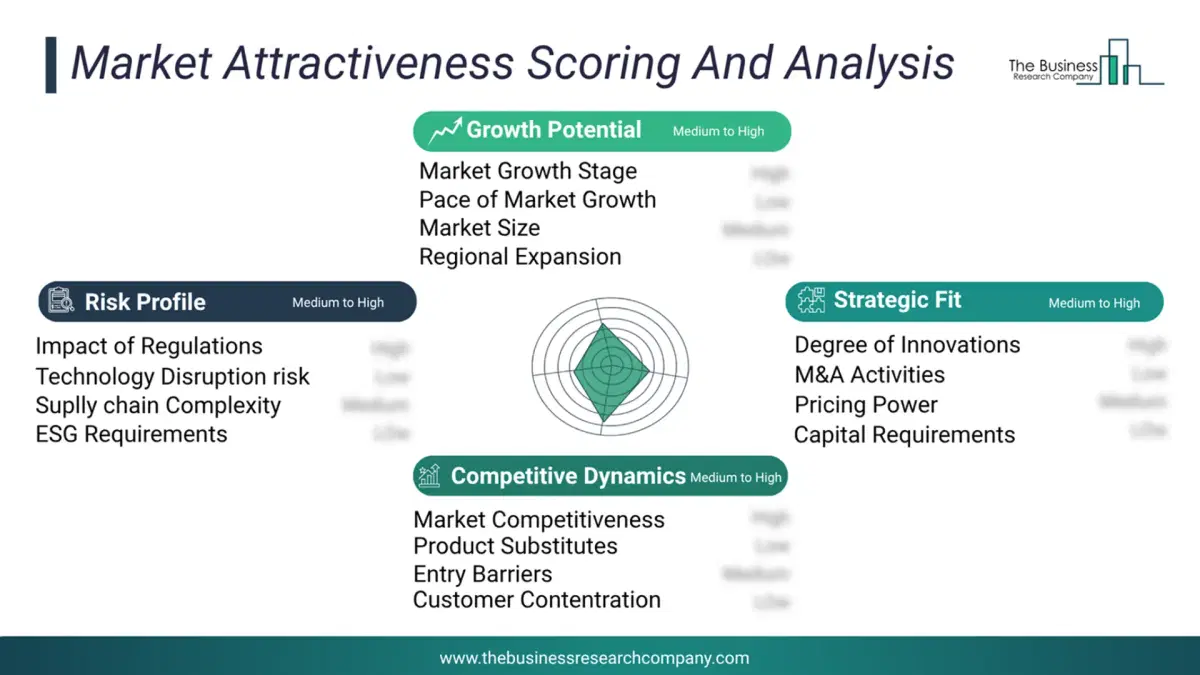
This chart presents market attractiveness based on a quantitative evaluation of growth, competition, strategic alignment, and risk, offering a clear view of opportunity areas for decision-making. This chart is for illustrative purposes; the full report contains the complete analysis.
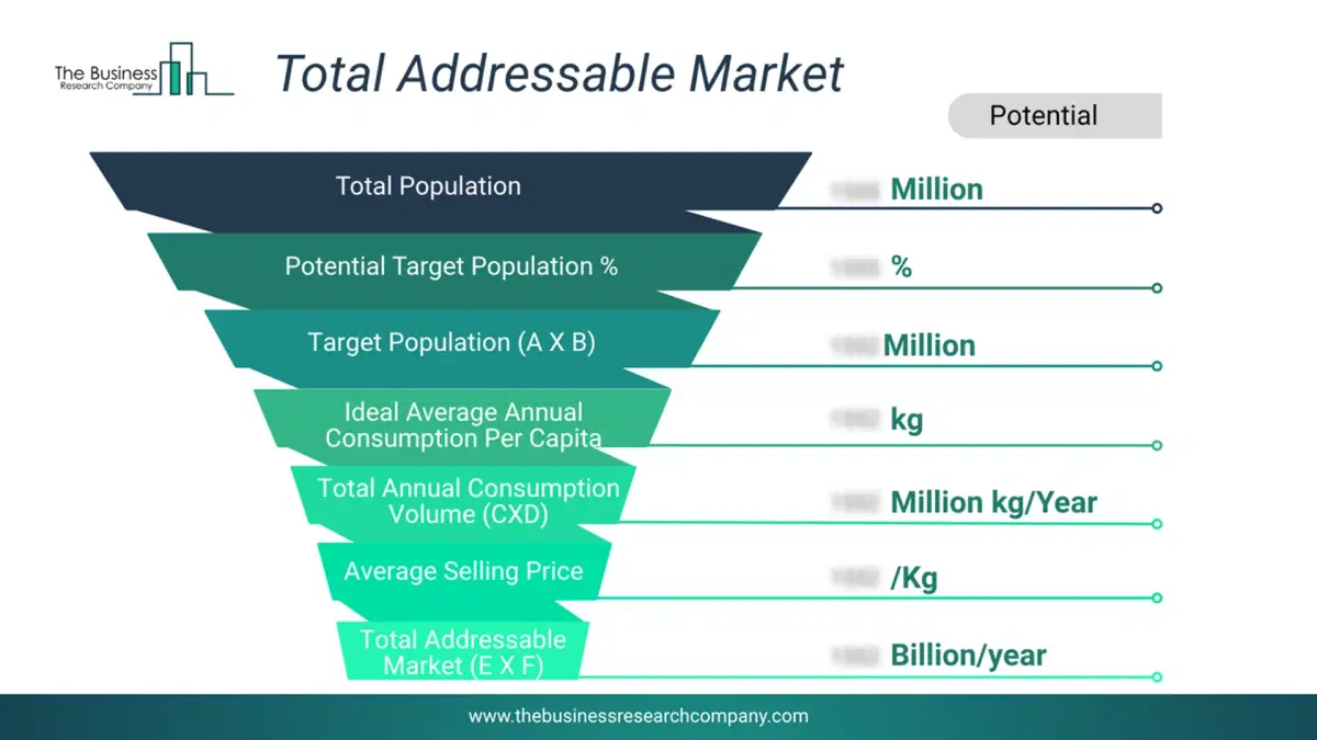
This chart highlights the Total Addressable Market (TAM) by estimating the maximum revenue opportunity using an assumption-driven approach, supporting strategic planning and opportunity sizing across markets. The chart is illustrative; the full report provides a more comprehensive analysis.
What Key Data and Analysis Are Included in the Semiconductor Packaging Market Report 2026?
The semiconductor packaging market research report is one of a series of new reports from The Business Research Company that provides semiconductor packaging market statistics, including semiconductor packaging industry global market size, regional shares, competitors with a semiconductor packaging market share, detailed semiconductor packaging market segments, market trends and opportunities, and any further data you may need to thrive in the semiconductor packaging industry. This semiconductor packaging market research report delivers a complete perspective of everything you need, with an in-depth analysis of the current and future scenario of the industry.Semiconductor Packaging Market Report Forecast Analysis
| Report Attribute | Details |
|---|---|
| Market Size Value In 2026 | $43.01 billion |
| Revenue Forecast In 2030 | $60.64 billion |
| Growth Rate | CAGR of 8.7% from 2026 to 2030 |
| Base Year For Estimation | 2025 |
| Actual Estimates/Historical Data | 2020-2025 |
| Forecast Period | 2026 - 2030 |
| Market Representation | Revenue in USD Billion and CAGR from 2026 to 2030 |
| Segments Covered | Packaging Type, Material, Technology, Application, End-Use |
| Regional Scope | Asia-Pacific, Western Europe, Eastern Europe, North America, South America, Middle East, Africa |
| Country Scope | The countries covered in the report are Australia, Brazil, China, France, Germany, India, Indonesia, Japan, Taiwan, Russia, South Korea, UK, USA, Canada, Italy, Spain. |
| Key Companies Profiled | Samsung Electronics Co. Ltd., Taiwan Semiconductor Manufacturing Company Ltd., Intel Corporation, ASE Technology Holding Co. Ltd., Amkor Technology Inc., JCET Group Co. Ltd., Siliconware Precision Industries Co. Ltd., Powertech Technology Inc., STATS ChipPAC Pte. Ltd., Tianshui Huatian Technology Co. Ltd., King Yuan Electronics Co. Ltd., UTAC Holdings Ltd., ChipMOS Technologies Inc., OSE Co. Ltd., Hana Micron Inc., Unisem (M) Berhad, Nepes Corporation, Formosa Advanced Technologies Co. Ltd., Walton Advanced Engineering Inc., AOI Electronics Co. Ltd., China Wafer Level CSP Co. Ltd., Tongfu Microelectronics Co. Ltd., Chipbond Technology Corporation, and Cactus Materials Inc. |
| Customization Scope | Request for Customization |
| Pricing And Purchase Options | Explore Purchase Options |