
Semiconductor Silicon Wafer Market Report 2026
Global Outlook – By Product Type (Prime Or Device Ready Wafers, Test Wafers, Reclaimed Wafers, Dummy Wafers), By Technology Node Type (Mature Nodes (Greater Than 28 Nanometers), Advanced Nodes (28 Nanometers To 10 Nanometers), Leading Edge Nodes (Less Than 10 Nanometers)), By Wafer Diameter Type (300 Millimeters (12 Inch), 200 Millimeters (8 Inch), 150 Millimeters And Below (6 Inch And Smaller)), By Application Type (Integrated Circuits, Discrete Semiconductors, Micro Electro Mechanical Systems Devices, Power Devices, Sensors, Optoelectronics, Analog Devices), By End Use Industry Type (Consumer Electronics, Automotive, Information Technology And Telecommunications, Industrial, Healthcare, Aerospace And Defense, Energy And Power) – Market Size, Trends, Strategies, and Forecast to 2030
Semiconductor Silicon Wafer Market Overview
• Semiconductor Silicon Wafer market size has reached to $14.12 billion in 2025 • Expected to grow to $21.71 billion in 2030 at a compound annual growth rate (CAGR) of 8.9% • Growth Driver: Rising Consumer Electronics Demand Driving The Market Growth Due To Rapid Digitalization And Smart Device Adoption • Market Trend: Expansion Of Advanced 300 Mm Wafer Fabrication Facilities To Enhance Semiconductor Manufacturing Efficiency • Asia-Pacific was the largest region and fastest growing region.What Is Covered Under Semiconductor Silicon Wafer Market?
A semiconductor silicon wafer is a thin, circular slice of highly purified crystalline silicon that serves as the foundational substrate for manufacturing integrated circuits and microelectronic devices. It is used in semiconductor fabrication processes where complex electronic circuits are built by layering and patterning materials on its ultra-smooth surface. The main product types of semiconductor silicon wafer include prime or device ready wafers, test wafers, reclaimed wafers, and dummy wafers. Prime or device ready wafers refer to high-quality silicon substrates manufactured with strict specifications and surface properties for semiconductor device fabrication. These wafers are produced for technology nodes including mature nodes (greater than 28 nanometers), advanced nodes (28 nanometers to 10 nanometers), and leading edge nodes (less than 10 nanometers) and are available in wafer diameters such as 300 millimeters (12 inch), 200 millimeters (8 inch), and 150 millimeters and below (6 inch and smaller). The various applications involved are integrated circuits, discrete semiconductors, micro electro mechanical systems devices, power devices, sensors, optoelectronics, and analog devices, and they are utilized by end-use industry types including consumer electronics, automotive, information technology and telecommunications, industrial, healthcare, aerospace and defense, and energy and power.
What Is The Semiconductor Silicon Wafer Market Size and Share 2026?
The semiconductor silicon wafer market size has grown strongly in recent years. It will grow from $14.12 billion in 2025 to $15.43 billion in 2026 at a compound annual growth rate (CAGR) of 9.3%. The growth in the historic period can be attributed to growing semiconductor manufacturing activities worldwide, increasing demand for integrated circuits across industries, rising adoption of electronic consumer devices, expanding semiconductor fabrication capacity, increasing requirement for high quality wafer substrates.What Is The Semiconductor Silicon Wafer Market Growth Forecast?
The semiconductor silicon wafer market size is expected to see strong growth in the next few years. It will grow to $21.71 billion in 2030 at a compound annual growth rate (CAGR) of 8.9%. The growth in the forecast period can be attributed to increasing demand for advanced semiconductor chips, rising investments in semiconductor fabrication plants, growing adoption of electric vehicles and smart devices, expanding production of advanced technology nodes, increasing demand for high performance computing applications. Major trends in the forecast period include increasing demand for advanced semiconductor silicon wafers, growing adoption of larger diameter silicon wafers, rising focus on high purity and defect free wafer production, expanding development of advanced semiconductor manufacturing processes, increasing investment in domestic semiconductor fabrication facilities.

Global Semiconductor Silicon Wafer Market Segmentation
2) By Technology Node Type: Mature Nodes (Greater Than 28 Nanometers), Advanced Nodes (28 Nanometers To 10 Nanometers), Leading Edge Nodes (Less Than 10 Nanometers) 3) By Wafer Diameter Type: 300 Millimeters (12 Inch), 200 Millimeters (8 Inch), 150 Millimeters And Below (6 Inch And Smaller) 4) By Application Type: Integrated Circuits, Discrete Semiconductors, Micro Electro Mechanical Systems Devices, Power Devices, Sensors, Optoelectronics, Analog Devices 5) By End Use Industry Type: Consumer Electronics, Automotive, Information Technology And Telecommunications, Industrial, Healthcare, Aerospace And Defense, Energy And Power Subsegments: 1) By Prime Or Device Ready Wafers: Monocrystalline Silicon Wafers, Polished Silicon Wafers, Epitaxial Silicon Wafers 2) By Test Wafers: Engineering Validation Wafers, Process Monitoring Wafers, Calibration Wafers 3) By Reclaimed Wafers: Reprocessed Silicon Wafers, Recycled Silicon Wafers, Polished Reused Wafers 4) By Dummy Wafers: Handling Wafers, Carrier Wafers, Spacer WafersWhat Are The Drivers Of The Semiconductor Silicon Wafer Market?
The rising demand for consumer electronics is expected to propel the growth of the semiconductor silicon wafer market going forward. Consumer electronics are mass-produced electronic devices intended for everyday personal use, including communication, entertainment, and home applications. Consumer electronics are rising due to growing demand for smart connected devices that enhance convenience, communication, and digital lifestyles. Semiconductor silicon wafers enable the production of advanced microchips that power consumer electronics, supporting faster performance, energy efficiency, and compact device designs. For instance, in May 2023, according to the Japan Electronics and Information Technology Industries Association, a Japan-based trade association, the total consumer electronic equipment production in Japan reached $209.16 million (¥32,099 million), compared to $164.65 million (¥25,268 million) in May 2022. Therefore, the rising demand for consumer electronics is driving the growth of the semiconductor silicon wafer industry. The growth in data centers and AI workloads is expected to propel the growth of the semiconductor silicon wafer market going forward. Data centers are centralized computing hubs that run and manage digital services, and AI workloads are the complex processing tasks for training and deploying artificial intelligence models on those systems. Data centers and AI workloads are increasing due to the rapid growth of digital data from cloud services and AI-driven applications that require large-scale storage and computing power. Semiconductor silicon wafers enable data centers and AI workloads by serving as the base material for manufacturing high-performance chips (CPUs, GPUs, and AI accelerators) that provide the computing power needed to process, store, and analyze massive amounts of data efficiently. For instance, in June 2025, according to EIDA Solutions, an Ireland-based software company, in 2024, data center planning applications in the UK surged by more than 40%, with Microsoft committing $3.2 billion (£2.5 billion) to double the nation’s AI infrastructure capacity by 2026. Therefore, the growth in data centers and AI workloads is driving the growth of the semiconductor silicon wafer industry.Key Players In The Global Semiconductor Silicon Wafer Market
Major companies operating in the semiconductor silicon wafer market are GlobalWafers Co. Ltd., Hebei Puxing Electronic Technology Co. Ltd., MCL Electronic Materials Co. Ltd., Nanjing Guosheng Electronics Co. Ltd., Nano Quarz Wafer GmbH, National Silicon Industry Group Co. Ltd., Okmetic Oy, RS Technologies Co. Ltd., Shanghai Simgui Technology Co. Ltd., Shin-Etsu Chemical Co. Ltd., Siltronic AG, SK Siltron Co. Ltd., Soitec SA, SUMCO Corporation, Wafer Works Corporation, WaferPro LLC.
This chart is for illustrative purposes; the full report includes a detailed competitor analysis and comprehensive overview of the top 10 companies in the market.

This chart maps companies by product innovation and brand strength, with bubble size indicating relative revenue, helping identify market leaders, challengers, and niche players. This is an illustrative chart; the full report provides a complete and accurate competitive analysis.
Global Semiconductor Silicon Wafer Market Trends and Insights
Major companies operating in the silicon wafer semiconductor market are focusing on developing innovative solutions, such as a 300 mm silicon wafer fabrication facility, to increase production efficiency, enhance chip performance, and meet the rising demand for advanced semiconductors. A 300 mm silicon wafer fabrication facility is a semiconductor plant that manufactures chips on 300 mm diameter silicon wafers to improve production efficiency and reduce cost per chip. For instance, in June 2024, Siltronic AG, a Germany-based manufacturer of wafers made of hyperpure silicon, launched an advanced wafer fabrication plant in Singapore to expand its global production capacity and strengthen supply chain resilience. The facility is equipped with state-of-the-art manufacturing technologies to ensure high-purity 300 mm wafer output and improved process precision. It is also designed to support next-generation semiconductor applications, including AI, automotive electronics, and high-performance computing.
Regional Outlook/Insights
Asia-Pacific was the largest region in the semiconductor silicon wafer market in 2025. Asia-Pacific is expected to be the fastest-growing region in the forecast period. The regions covered in this market report are Asia-Pacific, South East Asia, Western Europe, Eastern Europe, North America, South America, Middle East, Africa. The countries covered in this market report are Australia, Brazil, China, France, Germany, India, Indonesia, Japan, Taiwan, Russia, South Korea, UK, USA, Canada, Italy, Spain.What Defines the Semiconductor Silicon Wafer Market?
The semiconductor silicon wafer market consists of sales of polished wafers, doped wafers, and annealed wafers. Values in this market are ‘factory gate’ values, that is, the value of goods sold by the manufacturers or creators of the goods, whether to other entities (including downstream manufacturers, wholesalers, distributors, and retailers) or directly to end customers. The value of goods in this market includes related services sold by the creators of the goods.How is Market Value Defined and Measured?
The market value is defined as the revenues that enterprises gain from the sale of goods and/or services within the specified market and geography through sales, grants, or donations in terms of the currency (in USD unless otherwise specified). The revenues for a specified geography are consumption values that are revenues generated by organizations in the specified geography within the market, irrespective of where they are produced. It does not include revenues from resales along the supply chain, either further along the supply chain or as part of other products.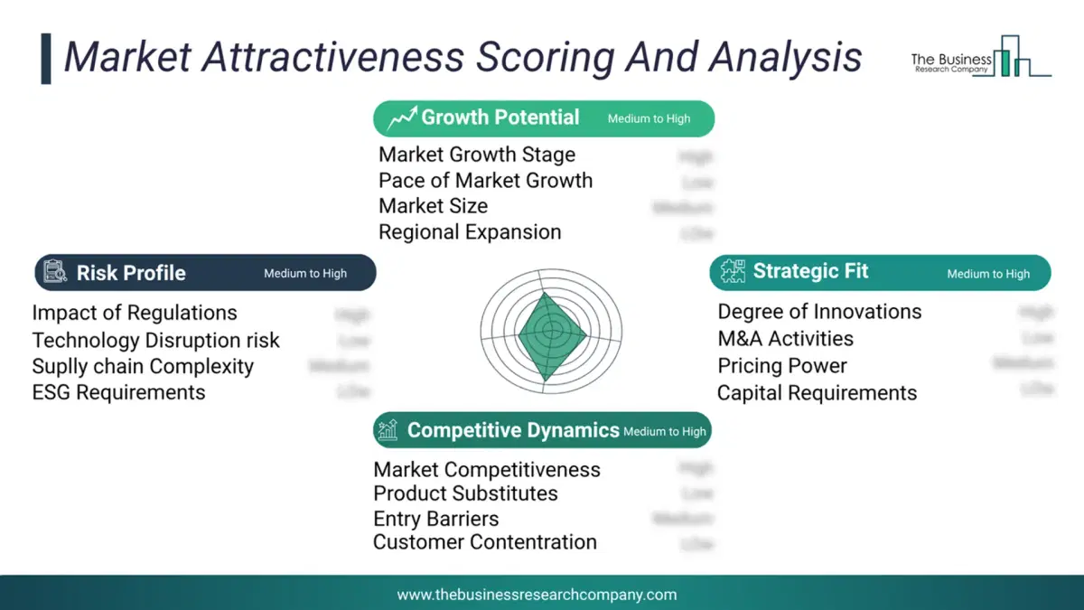
This chart presents market attractiveness based on a quantitative evaluation of growth, competition, strategic alignment, and risk, offering a clear view of opportunity areas for decision-making. This chart is for illustrative purposes; the full report contains the complete analysis.
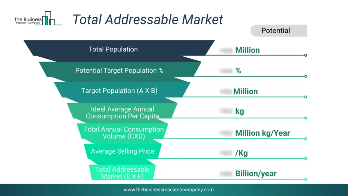
This chart highlights the Total Addressable Market (TAM) by estimating the maximum revenue opportunity using an assumption-driven approach, supporting strategic planning and opportunity sizing across markets. The chart is illustrative; the full report provides a more comprehensive analysis.
What Key Data and Analysis Are Included in the Semiconductor Silicon Wafer Market Report 2026?
The semiconductor silicon wafer market research report is one of a series of new reports from The Business Research Company that provides semiconductor silicon wafer market statistics, including semiconductor silicon wafer industry global market size, regional shares, competitors with a semiconductor silicon wafer market share, detailed semiconductor silicon wafer market segments, market trends and opportunities, and any further data you may need to thrive in the semiconductor silicon wafer industry. This semiconductor silicon wafer market research report delivers a complete perspective of everything you need, with an in-depth analysis of the current and future scenario of the industry.Semiconductor Silicon Wafer Market Report Forecast Analysis
| Report Attribute | Details |
|---|---|
| Market Size Value In 2026 | $15.43 billion |
| Revenue Forecast In 2030 | $21.71 billion |
| Growth Rate | CAGR of 8.9% from 2026 to 2030 |
| Base Year For Estimation | 2025 |
| Actual Estimates/Historical Data | 2020-2025 |
| Forecast Period | 2026 - 2030 |
| Market Representation | Revenue in USD Billion and CAGR from 2026 to 2030 |
| Segments Covered | Product Type, Technology Node Type, Wafer Diameter Type, Application Type, End Use Industry Type |
| Regional Scope | Asia-Pacific, Western Europe, Eastern Europe, North America, South America, Middle East, Africa |
| Country Scope | The countries covered in the report are Australia, Brazil, China, France, Germany, India, Indonesia, Japan, Taiwan, Russia, South Korea, UK, USA, Canada, Italy, Spain. |
| Key Companies Profiled | GlobalWafers Co. Ltd., Hebei Puxing Electronic Technology Co. Ltd., MCL Electronic Materials Co. Ltd., Nanjing Guosheng Electronics Co. Ltd., Nano Quarz Wafer GmbH, National Silicon Industry Group Co. Ltd., Okmetic Oy, RS Technologies Co. Ltd., Shanghai Simgui Technology Co. Ltd., Shin-Etsu Chemical Co. Ltd., Siltronic AG, SK Siltron Co. Ltd., Soitec SA, SUMCO Corporation, Wafer Works Corporation, WaferPro LLC. |
| Customization Scope | Request for Customization |
| Pricing And Purchase Options | Explore Purchase Options |