
Semiconductor Wafer Market Report 2026
Global Outlook – By Product ( Processor, Memory, Analog, Other Products), By Technology ( Wafer Bumping, Packaging And Assembly, Testing And Inspection, Other Technologies), By Application ( Consumer Electronics, Industrial, Telecommunication, Automotive, Other Applications) – Market Size, Trends, Strategies, and Forecast to 2030
Semiconductor Wafer Market Overview
• Semiconductor Wafer market size has reached to $17.48 billion in 2025 • Expected to grow to $22.88 billion in 2030 at a compound annual growth rate (CAGR) of 5.6% • Growth Driver: Rising Consumer Electronics Demand Fuels Growth Of Semiconductor Wafer Market • Market Trend: Advancements in Silicon Wafer Development to Meet Growing Industry Demands • Asia-Pacific was the largest region and fastest growing region.Market Gains By 2030 – Top Opportunities By Segment
Market Gain identifies the most promising market opportunities by highlighting the segments or products expected to generate the highest incremental revenue growth over the next five years.
What Is Covered Under Semiconductor Wafer Market?
Semiconductor wafer refers to a thin slice of semiconductor material, such as silicon, on which electronic circuits are fabricated. These wafers serve as the substrate on which microelectronic devices are built through processes such as doping, ion implantation, etching, and deposition of various materials. The main products of semiconductor wafer are processor, memory, analog, and others. Processor refers to the central processing unit (CPU) of a computer or electronic device responsible for executing instructions and performing calculations to carry out tasks. They are made of various technologies including wafer bumping, packaging and assembly, testing and inspection, and others for consumer electronics, industrial, telecommunication, automotive, and others.
What Is The Semiconductor Wafer Market Size 2026 And Growth Rate?
The semiconductor wafer market size has grown strongly in recent years. It will grow from $17.48 billion in 2025 to $18.42 billion in 2026 at a compound annual growth rate (CAGR) of 5.4%. The growth in the historic period can be attributed to growth of consumer electronics demand, expansion of semiconductor fabs, increasing miniaturization of electronic devices, early adoption of silicon based wafers, rising demand for memory and logic ICs.What Is The Semiconductor Wafer Market Growth Forecast?
The semiconductor wafer market size is expected to see strong growth in the next few years. It will grow to $22.88 billion in 2030 at a compound annual growth rate (CAGR) of 5.6%. The growth in the forecast period can be attributed to growth in EV and power electronics demand, expansion of AI and high performance computing, rising adoption of 5g and telecom infrastructure, increasing investments in advanced wafer fabs, demand for wide bandgap semiconductors. Major trends in the forecast period include increasing demand for advanced node semiconductor wafers, rising adoption of larger diameter wafers (300mm and beyond), growing focus on high yield and defect reduction, expansion of specialty wafers for power and rf devices, increasing use of advanced doping and deposition techniques.

Global Semiconductor Wafer Market Segmentation
1) By Product: Processor, Memory, Analog, Other Products 2) By Technology: Wafer Bumping, Packaging And Assembly, Testing And Inspection, Other Technologies 3) By Application: Consumer Electronics, Industrial, Telecommunication, Automotive, Other Applications Subsegments: 1) By Processor: Central Processing Unit (CPU) Wafers, Graphics Processing Unit (GPU) Wafers, System On Chip (SoC) Wafers, Microcontroller Unit (MCU) Wafers 2) By Memory: Dynamic Random Access Memory (DRAM) Wafers, Flash Memory Wafers (NAND, NOR), Static Random Access Memory (SRAM) Wafers, Read-Only Memory (ROM) Wafers 3) By Analog: Operational Amplifiers (Op-Amps), Power Management ICs (PMICs), Signal Processors, Voltage Regulators, Radio Frequency (RF) Chips 4) By Other Products: Optoelectronics (LED, Laser Diodes), Sensors (Temperature, Pressure, Image Sensors), Power Devices (MOSFETs, Diodes), MEMS (Micro-Electro-Mechanical Systems), Photonic Devices ( Potodiodes, modulators) The top segments in the semiconductor wafer market will be: • Memory will reach $8.02 Billion by 2030. • Processor will reach $6.84 Billion by 2030. • Analog will reach $4.5 Billion by 2030. • Other Products will reach $3.34 Billion by 2030.What Is The Driver Of The Semiconductor Wafer Market?
The increasing demand for consumer electronics is expected to propel the growth of the semiconductor wafer market going forward. Consumer electronics refer to electronic devices intended for everyday use by individuals. Consumer electronics constantly evolve with new and improved technologies, features, and functionalities, often providing convenience and improving productivity in various aspects of life. The semiconductor wafer is used in consumer electronics as the foundational substrate on which integrated circuits and microchips are fabricated, enabling the functionality of devices such as smartphones, computers, and televisions. For instance, in May 2023, according to the Japan Electronics and Information Technology Industries Association, a Japan-based trade association, the total electronic equipment production in Japan reached 771,457 units. In addition, consumer electronics production reached 32,099 units in May 2023, compared to 25,268 units in May 2022. Therefore, the increasing demand for consumer electronics is driving the growth of the semiconductor wafer industry.
Infographic Chart Showing Key Market Drivers Analysis And Restraints For Semiconductor Wafer Market
The chart presents an impact analysis of key drivers and restraints, quantifying their relative influence on the market's growth rate and helping assess the balance between growth enablers and limiting factors. This chart offers a high-level perspective; the full report contains more detailed insights.
How Will The Drivers Impact Growth In The Global Semiconductor Wafer Market?
• Rising Demand For 300 mm Wafers From Advanced Logic Fabs (High) – During the forecast period, the rising demand for 300 mm wafers from advanced logic fabs is expected to become a key growth driver for the semiconductor wafer market by 2030. Rising demand for 300 mm wafers from advanced logic fabs acts as a strong driver for the semiconductor wafer market by enabling higher chip production efficiency and scalability. These wafers allow manufacturers to produce more chips per cycle, reducing cost per unit and improving overall profitability. As advanced nodes require larger wafer sizes for optimal fabrication, leading foundries are increasingly transitioning toward 300 mm platforms. This shift is further supported by the need for high-performance computing, artificial intelligence, and data center applications. Additionally, 300 mm wafers enhance process uniformity and yield, making them more attractive for mass production. Investments in new fabrication facilities are also aligned with 300 mm wafer adoption, boosting demand. Consequently, the expansion of advanced logic fabs directly accelerates the growth of the semiconductor wafer market. • Increasing Deployment Of 5G Technology (High) – During the forecast period, the increasing deployment of 5g technology is expected to emerge as a major factor driving the expansion of the semiconductor wafer market by 2030. Increasing deployment of 5G technology significantly drives the semiconductor wafer market by creating massive demand for high-frequency and high-performance chips. 5G infrastructure requires advanced semiconductors for base stations, antennas, and network equipment, all of which depend on high-quality wafers. The proliferation of 5G-enabled devices such as smartphones, IoT devices, and connected systems further amplifies wafer consumption. Additionally, 5G technology demands faster processing speeds and lower latency, encouraging the production of advanced semiconductor nodes. This leads to increased utilization of silicon wafers in manufacturing processes. Telecom operators and governments worldwide are heavily investing in 5G rollout, sustaining long-term demand. As a result, the continuous expansion of 5G networks directly fuels growth in the semiconductor wafer market. • Increasing Demand For Semiconductor Devices (High) – During the forecast period, the increasing demand for semiconductor devices is expected to act as a key growth catalyst for the semiconductor wafer market by 2030. Increasing demand for semiconductor devices serves as a fundamental driver for the semiconductor wafer market by expanding the overall consumption of electronic components. The growing adoption of consumer electronics, automotive electronics, and industrial automation systems has intensified the need for semiconductors. Emerging technologies such as artificial intelligence, cloud computing, and electric vehicles further contribute to rising chip demand. As semiconductors are manufactured using silicon wafers, any increase in device production directly boosts wafer demand. Moreover, the trend toward miniaturization and enhanced performance requires more sophisticated wafer processing. Global digital transformation initiatives are also accelerating semiconductor usage across industries. Therefore, the rising demand for semiconductor devices consistently propels the growth of the semiconductor wafer market.How Will The Restraints Impact Growth In The Global Semiconductor Wafer Market?
• Ultra-Flat 300 mm Capex And Yield Challenges (High) – During the forecast period, the ultra-flat 300 mm capex and yield challenges act as a restraint on the semiconductor wafer market by increasing the financial burden on manufacturers. The production of ultra-flat wafers requires highly advanced equipment and precision engineering, leading to significant capital expenditure. Smaller manufacturers often struggle to afford these investments, limiting market participation and competition. Additionally, achieving consistent wafer flatness is technically complex and can result in yield losses during fabrication. Lower yields directly impact profitability and operational efficiency. Continuous process optimization is required, which further raises operational costs and time. As a result, these challenges slow down capacity expansion and hinder the overall growth of the semiconductor wafer market. • Quartz Crucible And Polysilicon Purity Bottlenecks (High) – During the forecast period, the quartz crucible and polysilicon purity bottlenecks restrict the semiconductor wafer market by disrupting the supply chain of critical raw materials. High-purity polysilicon is essential for producing defect-free wafers, and any limitation in its availability affects production volumes. Similarly, quartz crucibles used in crystal growth must meet stringent quality standards, making their supply highly specialized. Shortages or inconsistencies in these materials can lead to production delays and increased defect rates. Manufacturers may face higher procurement costs due to limited suppliers and rising demand. This also impacts the scalability of wafer production, especially during peak demand periods. Consequently, material bottlenecks create significant constraints on market growth and stability. • Ongoing Global Shortage Of Semiconductor Chips (High) – During the forecast period, the ongoing global shortage of semiconductor chips acts as a restraint by creating imbalances across the semiconductor wafer market. While demand for wafers rises, supply chain disruptions prevent manufacturers from fully capitalizing on this demand. Factors such as geopolitical tensions, logistics disruptions, and limited fabrication capacity contribute to the shortage. This leads to extended lead times and uncertainty in production planning. Wafer manufacturers may struggle to align supply with fluctuating chip demand from various industries. Additionally, shortages can cause price volatility, affecting both suppliers and end users. As a result, the persistent chip shortage creates instability and limits the steady growth of the semiconductor wafer market.Key Players In The Global Semiconductor Wafer Market
Major companies operating in the semiconductor wafer market are Samsung Electronics, Intel Corporation, Qualcomm Incorporated, ASML Holding, LONGi Green Energy Technology Co. Ltd., Shin-Etsu Chemical Co. Ltd., Tokyo Electron Limited, STMicroelectronics N.V., KLA Corporation, Microchip Technology Inc., SUMCO Corporation, Globalwafers, Siltronic AG, Soitec, Fujimi Incorporated, Wafer Works Corporation, Ferrotec Holdings Corporation, Okmetic Inc., Episil-Precision Inc., Alfa Chemistry, ShanghAI Simgui Technology Co. Ltd., SK Siltron Co. Ltd., Wafer World Inc., WaferPro, Virginia Semiconductor
This chart is for illustrative purposes; the full report includes a detailed competitor analysis and comprehensive overview of the top 10 companies in the market.

This chart maps companies by product innovation and brand strength, with bubble size indicating relative revenue, helping identify market leaders, challengers, and niche players. This is an illustrative chart; the full report provides a complete and accurate competitive analysis.
Global Semiconductor Wafer Market Trends and Insights
Major companies operating in the semiconductor wafer market are developing silicon wafers to meet the increasing demand for advanced electronic devices in various industries. Silicon wafers serve as the substrate for fabricating integrated circuits (ICs) and semiconductor devices. For instance, in April 2024, LONGi, a China-based photovoltaics company, launched TaiRay silicon wafer products. The TaiRay silicon wafers are designed to support multiple cell technologies and are available in various sizes and thicknesses to meet different market needs. TaiRay wafers also have enhanced mechanical properties, with a 16% higher bending strength than conventional wafers. This increased bending strength helps reduce the breakage rate during production, mainly when producing thinner wafers.What Are Latest Mergers And Acquisitions In The Semiconductor Wafer Market?
In September 2023, Robert Bosch GmbH, a Germany-based engineering and technology company, acquired TSI Semiconductors Corporation for an undisclosed amount. With this acquisition, Bosch significantly expanded its manufacturing capacity for silicon carbide (SiC) chips, enhanced its global semiconductor portfolio, strengthened its presence in the North American market, and reinforced its commitment to advancing electromobility and high-efficiency electronic solutions. TSI Semiconductors Corporation is a US-based semiconductor company that designs and produces semiconductor wafers for various applications, including automotive and industrial sectors.
Regional Outlook
Asia-Pacific was the largest region in the semiconductor wafer market in 2025. Asia-Pacific is expected to be the fastest-growing region in the forecast period. The regions covered in this market report are Asia-Pacific, South East Asia, Western Europe, Eastern Europe, North America, South America, Middle East, Africa. The countries covered in this market report are Australia, Brazil, China, France, Germany, India, Indonesia, Japan, Taiwan, Russia, South Korea, UK, USA, Canada, Italy, Spain.What Defines the Semiconductor Wafer Market?
The semiconductor wafer market consists of sales of silicon wafer, photolithography machines, wafer cleaning systems, dicing machines, optical microscopes, and wafer carriers and cassettes. Values in this market are ‘factory gate’ values, that is the value of goods sold by the manufacturers or creators of the goods, whether to other entities (including downstream manufacturers, wholesalers, distributors and retailers) or directly to end customers. The value of goods in this market includes related services sold by the creators of the goods.How is Market Value Defined and Measured?
The market value is defined as the revenues that enterprises gain from the sale of goods and/or services within the specified market and geography through sales, grants, or donations in terms of the currency (in USD unless otherwise specified). The revenues for a specified geography are consumption values that are revenues generated by organizations in the specified geography within the market, irrespective of where they are produced. It does not include revenues from resales along the supply chain, either further along the supply chain or as part of other products.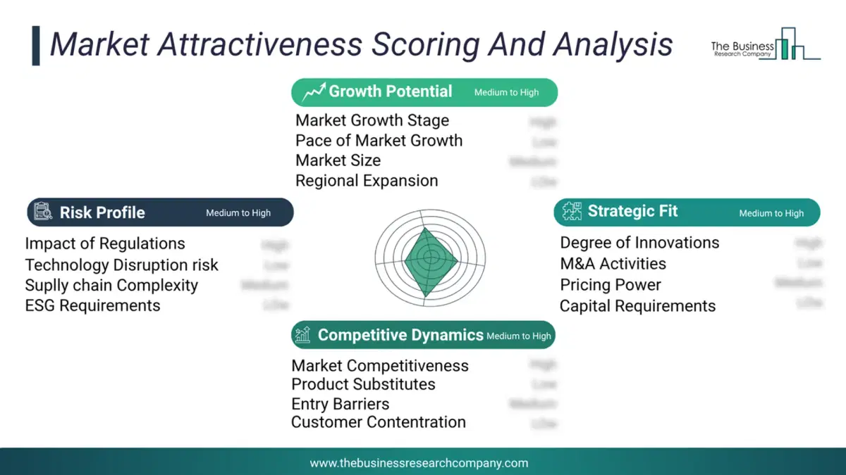
This chart presents market attractiveness based on a quantitative evaluation of growth, competition, strategic alignment, and risk, offering a clear view of opportunity areas for decision-making. This chart is for illustrative purposes; the full report contains the complete analysis.
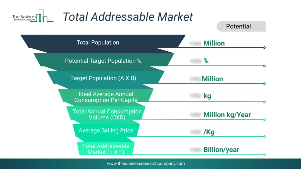
This chart highlights the Total Addressable Market (TAM) by estimating the maximum revenue opportunity using an assumption-driven approach, supporting strategic planning and opportunity sizing across markets. The chart is illustrative; the full report provides a more comprehensive analysis.
What Key Data and Analysis Are Included in the Semiconductor Wafer Market Report 2026?
The semiconductor wafer market research report is one of a series of new reports from The Business Research Company that provides market statistics, including industry global market size, regional shares, competitors with the market share, detailed market segments, market trends and opportunities, and any further data you may need to thrive in the semiconductor wafer industry. The market research report delivers a complete perspective of everything you need, with an in-depth analysis of the current and future state of the industry.Semiconductor Wafer Market Report Forecast Analysis Market Report Forecast Analysis
| Report Attribute | Details |
|---|---|
| Market Size Value In 2026 | $18.42 billion |
| Revenue Forecast In 2030 | $22.88 billion |
| Growth Rate | CAGR of 5.4% from 2026 to 2030 |
| Base Year For Estimation | 2025 |
| Actual Estimates/Historical Data | 2020-2025 |
| Forecast Period | 2026 - 2030 |
| Market Representation | Revenue in USD Billion and CAGR from 2026 to 2030 |
| Segments Covered | Product, Technology, Application |
| Regional Scope | Asia-Pacific, Western Europe, Eastern Europe, North America, South America, Middle East, Africa |
| Country Scope | The countries covered in the report are Australia, Brazil, China, France, Germany, India, Indonesia, Japan, Taiwan, Russia, South Korea, UK, USA, Canada, Italy, Spain. |
| Key Companies Profiled | Samsung Electronics, Intel Corporation, Qualcomm Incorporated, ASML Holding, LONGi Green Energy Technology Co. Ltd., Shin-Etsu Chemical Co. Ltd., Tokyo Electron Limited, STMicroelectronics N.V., KLA Corporation, Microchip Technology Inc., SUMCO Corporation, Globalwafers, Siltronic AG, Soitec, Fujimi Incorporated, Wafer Works Corporation, Ferrotec Holdings Corporation, Okmetic Inc., Episil-Precision Inc., Alfa Chemistry, ShanghAI Simgui Technology Co. Ltd., SK Siltron Co. Ltd., Wafer World Inc., WaferPro, Virginia Semiconductor |
| Customization Scope | Request for Customization |
| Pricing And Purchase Options | Explore Purchase Options |