

Thin Wafer Processing And Dicing Equipment Market Report 2026
Global Outlook – By Equipment Type (Dicing Equipment, Wafer Processing Equipment), By Wafer Thickness (750 Micrometer, 120 Micrometer, 50 Micrometer), By Wafer Size (200 Millimeter, 300 Millimeter, Other Wafer Sizes), By Application (Memory Devices, Logic Devices, Micro-Electro-Mechanical Systems, Power Devices, Radio-Frequency Identification, Complementary Metal-Oxide-Semiconductor Image Sensors, Other Applications), By End-User (Semiconductor Manufacturers, Foundries, Other End Users) – Market Size, Trends, Strategies, and Forecast to 2035
Thin Wafer Processing And Dicing Equipment Market Overview
• Thin Wafer Processing And Dicing Equipment market size has reached to $0.97 billion in 2025 • Expected to grow to $1.43 billion in 2030 at a compound annual growth rate (CAGR) of 8.2% • Growth Driver: Rising Adoption Of Consumer Electronics Is Fueling The Growth Of The Market Due To Increasing Demand For Compact, High-Performance, And Energy-Efficient Semiconductor Chips • Market Trend: Advancements In Laser Lift-Off Technology Enhance Processing Efficiency For Wafer-Bonded Devices • Asia-Pacific was the largest region and fastest growing region.What Is Covered Under Thin Wafer Processing And Dicing Equipment Market?
Thin wafer processing and dicing equipment refer to advanced semiconductor tools designed to support the handling, thinning, and precise cutting of silicon wafers into individual dies. Its primary purpose is to achieve accurate wafer thinning and separation, enabling the production of compact, high-performance electronic devices while enhancing packaging efficiency and reducing material waste and defects. The main equipment types of thin wafer processing and dicing equipment include dicing equipment and wafer processing equipment. Dicing equipment refers to precision systems used to cut semiconductor wafers into individual dies with high accuracy and minimal material loss. These solutions are based on wafer thickness such as 750 micrometer, 120 micrometer, and 50 micrometer and they are designed for wafer sizes including 200 millimeter, 300 millimeter, and other wafer sizes. The key applications involved are memory devices, logic devices, micro-electro-mechanical systems, power devices, radio-frequency identification, complementary metal-oxide-semiconductor image sensors, and other applications, and they are used by several end users such as semiconductor manufacturers, foundries, and other end users.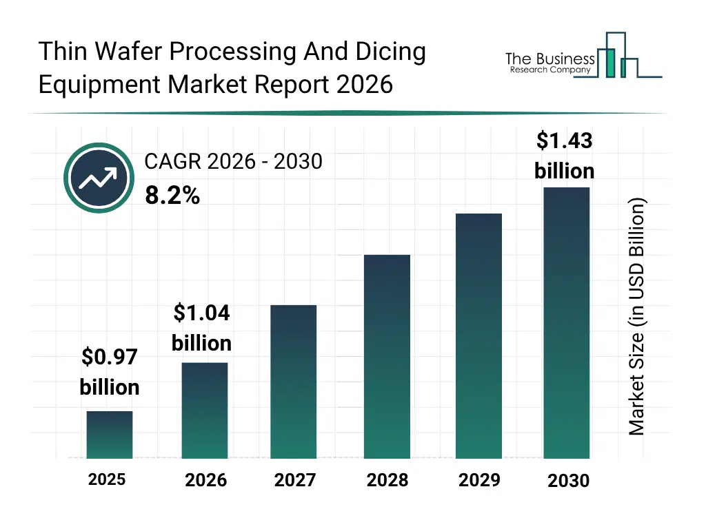
What Is The Thin Wafer Processing And Dicing Equipment Market Size and Share 2026?
The thin wafer processing and dicing equipment market size has grown strongly in recent years.It will grow from $0.97 billion in 2025 to $1.04 billion in 2026 at a compound annual growth rate (CAGR) of 7.9%. The growth in the historic period can be attributed to growing demand for miniaturized semiconductor devices, increasing adoption of advanced packaging technologies, expansion of consumer electronics manufacturing, rising investments in semiconductor fabrication facilities, increasing demand for high precision wafer processing equipment.What Is The Thin Wafer Processing And Dicing Equipment Market Growth Forecast?
The thin wafer processing and dicing equipment market size is expected to see strong growth in the next few years.It will grow to $1.43 billion by 2030 at a compound annual growth rate (CAGR) of 8.2%. The growth in the forecast period can be attributed to growing demand for AI and high-performance computing chips, rising adoption of electric vehicles and power semiconductors, increasing investment in next-generation semiconductor fabs, expansion of MEMS and CMOS image sensor production, growing innovation in automated laser and plasma dicing technologies.Major trends in the forecast period include increasing adoption of ultra-thin wafer processing technologies for compact semiconductor packaging, rising demand for precision laser dicing equipment to reduce wafer defects, growing use of automated wafer inspection systems for yield optimization, expanding development of low-damage wafer thinning technologies for advanced semiconductor devices, increasing integration of high-accuracy wafer cleaning and polishing equipment in semiconductor fabrication facilities.
Global Thin Wafer Processing And Dicing Equipment Market Segmentation
1) By Equipment Type: Dicing Equipment, Wafer Processing Equipment 2) By Wafer Thickness: 750 Micrometer, 120 Micrometer, 50 Micrometer 3) By Wafer Size: 200 Millimeter, 300 Millimeter, Other Wafer Sizes 4) By Application: Memory Devices, Logic Devices, Micro-Electro-Mechanical Systems, Power Devices, Radio-Frequency Identification, Complementary Metal-Oxide-Semiconductor Image Sensors, Other Applications 5) By End-User: Semiconductor Manufacturers, Foundries, Other End Users Subsegments: 1) By Dicing Equipment: Blade Dicing Equipment, Laser Dicing Equipment, Plasma Dicing Equipment, Stealth Dicing Equipment, Automatic Wafer Dicing Equipment 2) By Wafer Processing Equipment: Wafer Grinding Equipment, Wafer Polishing Equipment, Wafer Thinning Equipment, Wafer Cleaning Equipment, Wafer Inspection EquipmentWhat Are The Drivers Of The Thin Wafer Processing And Dicing Equipment Market?
The rising adoption of consumer electronics is expected to propel the growth of the thin wafer processing and dicing equipment industry going forward.Consumer electronics refer to electronic devices intended for daily use by individuals, including products such as smartphones, televisions, laptops, and home entertainment systems.The rising adoption of consumer electronics is driven by increasing disposable income, enabling higher spending on advanced devices and driving frequent upgrades, along with growing demand for innovative, feature-rich products.Thin wafer processing and dicing equipment enable the production of ultra-thin, high-performance chips for compact consumer electronics, improving efficiency, reducing power consumption, and enhancing device functionality.For instance, in May 2023, according to the Japan Electronics and Information Technology Industries Association, a Japan-based trade association, the total consumer electronic equipment production in Japan reached $209.16 million (¥32,099 million), compared to $164.65 million (¥25,268 million) in May 2022.Therefore, the rising adoption of consumer electronics is driving the growth of the thin wafer processing and dicing equipment industry. The expansion of the global semiconductor industry is expected to propel the growth of the thin wafer processing and dicing equipment industry going forward.The semiconductor industry refers to the sector involved in the design, manufacturing, and distribution of semiconductor devices and integrated circuits used in electronic products and systems.The expansion of the global semiconductor industry is driven by rising demand for advanced computing technologies, increasing adoption of artificial intelligence, 5G infrastructure deployment, and growing production of connected electronic devices.Thin wafer processing and dicing equipment support the semiconductor industry by enabling the production of thinner, high-performance semiconductor wafers that improve chip efficiency, reduce power consumption, and support miniaturization in advanced electronic applications.For instance, in February 2025, according to the Semiconductor Industry Association (SIA), a US-based trade association representing the semiconductor industry, global semiconductor sales reached approximately $627.6 billion in 2024, reflecting a 19.1% increase compared to 2023.Therefore, the expansion of the global semiconductor industry is driving the growth of the thin wafer processing and dicing equipment industry.Key Players In The Global Thin Wafer Processing And Dicing Equipment Market
Major companies operating in the thin wafer processing and dicing equipment market are Panasonic Connect Co. Ltd, Lam Research Corporation, KLA Corporation, Han's Laser Technology Industry Group Co. Ltd, DISCO Corporation, ASMPT Limited, Kulicke and Soffa Industries Inc, Veeco Instruments Inc, EV Group GmbH, SUSS MicroTec SE, MTI Corporation, Hanmi Semiconductor Co. Ltd, Plasma-Therm LLC, Tokyo Seimitsu Co. Ltd, AXUS Technology Inc, Yamamoto Manufacturing Co. Ltd, NeonTech Co. Ltd, Synova SA, Citizen Chiba Precision Co. Ltd, Dynatex International Inc, Suzhou Delphi Laser Co. Ltd, Loadpoint LimitedGlobal Thin Wafer Processing And Dicing Equipment Market Trends and Insights
Major companies operating in the thin wafer processing and dicing equipment market are focusing on developing advanced solutions, such as extreme laser lift-off systems, to improve precision, reduce material damage, and enhance processing efficiency for wafer-bonded devices. Laser lift-off refers to a technology used to separate thin semiconductor layers from carrier substrates using high-energy laser pulses, enabling the fabrication of ultra-thin and high-performance devices. For instance, in December 2024, Tokyo Electron, a Japan-based semiconductor equipment manufacturer, launched Ulucus LX, an extreme laser lift-off system designed for 300 mm wafer-bonded devices. The system enables high-throughput and damage-free separation of bonded wafers, supporting advanced semiconductor packaging and improving overall device performance and manufacturing efficiency.Regional Insights
Asia-Pacific was the largest region in the thin wafer processing and dicing equipment market in 2025. Asia-Pacific is expected to be the fastest-growing region in the forecast period. The regions covered in this market report are Asia-Pacific, South East Asia, Western Europe, Eastern Europe, North America, South America, Middle East and Africa. The countries covered in this market report are Australia, Brazil, China, France, Germany, India, Indonesia, Japan, Taiwan, Russia, South Korea, UK, USA, Canada, Italy, Spain.What Defines the Thin Wafer Processing And Dicing Equipment Market?
The thin wafer processing and dicing equipment market consists of sales of wafer thinning machines, precision dicing saws, and laser cutting systems. Values in this market are ‘factory gate’ values, that is, the value of goods sold by the manufacturers or creators of the goods, whether to other entities (including downstream manufacturers, wholesalers, distributors, and retailers) or directly to end customers. The value of goods in this market includes related services sold by the creators of the goods.What is the Market Assessment and Strategic Outlook for the Thin Wafer Processing And Dicing Equipment Industry?
The thin wafer processing and dicing equipment market research report is one of a series of new reports from The Business Research Company that provides market statistics, including industry global market size, regional shares, competitors with the market share, detailed market segments, market trends and opportunities, and any further data you may need to thrive in the thin wafer processing and dicing equipment industry. The market research report delivers a complete perspective of everything you need, with an in-depth analysis of the current and future state of the industry.What is the Market Assessment and Strategic Outlook for the Thin Wafer Processing And Dicing Equipment Market Report 2026?
The thin wafer processing and dicing equipment market research report is one of a series of new reports from The Business Research Company that provides thin wafer processing and dicing equipment market statistics, including thin wafer processing and dicing equipment industry global market size, regional shares, competitors with a thin wafer processing and dicing equipment market share, detailed thin wafer processing and dicing equipment market segments, market trends and opportunities, and any further data you may need to thrive in the thin wafer processing and dicing equipment industry. This thin wafer processing and dicing equipment market research report delivers a complete perspective of everything you need, with an in-depth analysis of the current and future scenario of the industry.Thin Wafer Processing And Dicing Equipment Market Report Forecast Analysis
| Report Attribute | Details |
|---|---|
| Market Size Value In 2026 | $1.04 billion |
| Revenue Forecast In 2035 | $1.43 billion |
| Growth Rate | CAGR of 8.2% from 2026 to 2035 |
| Base Year For Estimation | 2025 |
| Actual Estimates/Historical Data | 2020-2025 |
| Forecast Period | 2026 - 2030 - 2035 |
| Market Representation | Revenue in USD Billion and CAGR from 2026 to 2035 |
| Segments Covered | Equipment Type, Wafer Thickness, Wafer Size, Application, End-User |
| Regional Scope | Asia-Pacific, Western Europe, Eastern Europe, North America, South America, Middle East, Africa |
| Country Scope | The countries covered in the report are Australia, Brazil, China, France, Germany, India, Indonesia, Japan, Taiwan, Russia, South Korea, UK, USA, Canada, Italy, Spain. |
| Key Companies Profiled | Panasonic Connect Co. Ltd, Lam Research Corporation, KLA Corporation, Han's Laser Technology Industry Group Co. Ltd, DISCO Corporation, ASMPT Limited, Kulicke and Soffa Industries Inc, Veeco Instruments Inc, EV Group GmbH, SUSS MicroTec SE, MTI Corporation, Hanmi Semiconductor Co. Ltd, Plasma-Therm LLC, Tokyo Seimitsu Co. Ltd, AXUS Technology Inc, Yamamoto Manufacturing Co. Ltd, NeonTech Co. Ltd, Synova SA, Citizen Chiba Precision Co. Ltd, Dynatex International Inc, Suzhou Delphi Laser Co. Ltd, Loadpoint Limited |
| Customization Scope | Request for Customization |
| Pricing And Purchase Options | Explore Purchase Options |