

Silicon EPI Wafer Market Report 2026
Global Outlook – By Type ( Heteroepitaxy, Homoepitaxy), By Equipment ( Thermal Processing System, Etch System, Coater Or Developer, Surface Preparation System, Single Wafer Deposition, Wafer Bonder Or De-Bonder, Epitaxial CVD System, Ion Implantation System, Other Equipment), By Process Type ( CVD, Liquid Phase Epitaxy, Molecular Beam Epitaxy), By Reactors ( Pancake Reactor Or Horizontal Reactor, Barrel Reactor), By Industry Vertical ( Consumer Electronics, Automotive, Healthcare, Industrial, Other Industry Verticals) – Market Size, Trends, Strategies, and Forecast to 2030
Silicon EPI Wafer Market Overview
• Silicon EPI Wafer market size has reached to $1.89 billion in 2025 • Expected to grow to $2.52 billion in 2030 at a compound annual growth rate (CAGR) of 5.9% • Growth Driver: 5G Infrastructure Driving The Silicon Epi Wafer Market • Market Trend: Next-Generation Silicon EPI Wafers Revolutionize The Market • Asia-Pacific was the largest region and fastest growing region.Market Gains By 2030 – Top Opportunities By Segment
Market Gain identifies the most promising market opportunities by highlighting the segments or products expected to generate the highest incremental revenue growth over the next five years.
What Is Covered Under Silicon EPI Wafer Market?
Silicon EPI wafer is a semiconducting wafer that is used in the fabrication of integrated circuits. Silicon wafers are critical components used in the production of various semiconductor components. They are the fundamental building blocks for semiconductors, which are used in everything from the most miniature sensor in a light bulb to the most advanced electronic system, such as the space shuttle. The main types of silicon EPI wafers are heteroepitaxy and homoepitaxy. Heteroepitaxy is a type of heterogeneous nucleation in which the orientations of the substrate and the material deposited on it have a distinct crystallographic relationship. The equipment includes a thermal processing system, an etch system, a coater or developer, a surface preparation system, a single wafer deposition system, a wafer bonder or debonder, an epitaxial CVD system, an ion implantation system, and other equipment. The various processes include CVD, liquid-phase epitaxy, and molecular beam epitaxy. The various reactors include pancake reactors or horizontal and barrel reactors used in industry verticals including consumer electronics, automotive, healthcare, industrial, and others such as lighting and telecommunications.
What Is The Silicon EPI Wafer Market Size 2026 And Growth Rate?
The silicon epi wafer market size has grown strongly in recent years. It will grow from $1.89 billion in 2025 to $2 billion in 2026 at a compound annual growth rate (CAGR) of 6.2%. The growth in the historic period can be attributed to growth in consumer electronics chip demand, reliance on traditional silicon wafer production, early adoption of epitaxial wafers in automotive electronics, expansion of industrial and healthcare semiconductors, development of basic epitaxy processes.What Is The Silicon EPI Wafer Market Growth Forecast?
The silicon epi wafer market size is expected to see strong growth in the next few years. It will grow to $2.52 billion in 2030 at a compound annual growth rate (CAGR) of 5.9%. The growth in the forecast period can be attributed to increasing need for high-performance computing wafers, expansion of automotive and industrial chip applications, rising investment in advanced epitaxy equipment, development of next-generation heteroepitaxy solutions, growth in smart device manufacturing ecosystems. Major trends in the forecast period include expansion of advanced semiconductor manufacturing processes, adoption of epitaxial technologies for AI and high-performance chips, integration of smart wafer fabrication systems, development of high-purity epi structures for intelligent devices, advancement of automated deposition and process control.

Global Silicon EPI Wafer Market Segmentation
1) By Type: Heteroepitaxy, Homoepitaxy 2) By Equipment: Thermal Processing System, Etch System, Coater Or Developer, Surface Preparation System, Single Wafer Deposition, Wafer Bonder Or De-Bonder, Epitaxial CVD System, Ion Implantation System, Other Equipment 3) By Process Type: CVD, Liquid Phase Epitaxy, Molecular Beam Epitaxy 4) By Reactors: Pancake Reactor Or Horizontal Reactor, Barrel Reactor 5) By Industry Vertical: Consumer Electronics, Automotive, Healthcare, Industrial, Other Industry Verticals Subsegments: 1) By Heteroepitaxy: Silicon On Insulator (SOI) Wafers, Silicon-Germanium (SiGe) Wafers, Gallium Nitride (GaN) On Silicon Wafers 2) By Homoepitaxy: Standard Silicon Epitaxial Wafers, High-Quality Epitaxial Wafers, Low-Temperature Epitaxial Wafers The top segments in the silicon epi wafer market will be: • Homoepitaxy will reach $2 Billion by 2030. • Heteroepitaxy will reach $0.69 Billion by 2030.What Is The Driver Of The Silicon EPI Wafer Market?
The development of 5G infrastructure is expected to propel the growth of the silicon EPI wafer market going forward. 5G refers to a mobile network that is fifth-generation. Silicon EPI wafers play a crucial role in 5G infrastructure by enabling the production of high-frequency, high-performance semiconductor devices, such as RF amplifiers and switches, essential for the efficient and rapid transmission of 5G signals. For instance, in May 2023, according to Telefonaktiebolaget LM Ericsson, a Sweden-based information and communication technology company, it is expected that 4.624 billion 5G mobile subscriptions will be in place, up from 1.481 billion in 2023. Therefore, the development of 5G infrastructure is driving the silicon EPI wafer industry.
Infographic Chart Showing Key Market Drivers Analysis And Restraints For Silicon Epi Wafer Market
The chart presents an impact analysis of key drivers and restraints, quantifying their relative influence on the market's growth rate and helping assess the balance between growth enablers and limiting factors. This chart offers a high-level perspective; the full report contains more detailed insights.
How Will The Drivers Impact Growth In The Global Silicon EPI Wafer Market?
• Growing Demand From Semiconductor Industry (Low) – During the forecast period, the growing demand from the semiconductor industry is expected to emerge as a major factor driving the expansion of the silicon EPI wafer market by 2030. increasing production of integrated circuits, power semiconductors, MEMS devices, RF components, and image sensors, combined with investments in new semiconductor fabrication facilities, is generating sustained demand for high-quality epitaxial wafers with superior crystal characteristics. the expansion of AI, cloud computing, 5G infrastructure, industrial automation, and domestic chip manufacturing initiatives is further supporting market growth. • Increasing Adoption Of Consumer Electronics And Automotive Electronics (Medium) – During the forecast period, the increasing adoption of consumer electronics and automotive electronics is expected to emerge as a major factor driving the expansion of the silicon EPI wafer market by 2030. the continuous launch of smartphones, wearable devices, smart home products, and connected consumer electronics, together with the rapid electrification of vehicles and deployment of ADAS, infotainment systems, battery management systems, and automotive sensors, is significantly increasing semiconductor demand. this growing semiconductor content across electronic products is strengthening the requirement for advanced silicon epitaxial wafers. • Rising Demand For High-Performance And Energy-Efficient Devices (Medium) – During the forecast period, the rising demand for high-performance and energy-efficient devices is expected to act as a key growth catalyst for the silicon EPI wafer market by 2030. advanced semiconductor applications increasingly require wafers that deliver enhanced electrical performance, lower leakage current, higher breakdown voltage, and improved energy efficiency for processors, power devices, and communication chips. growing deployment of advanced computing systems, renewable energy technologies, healthcare electronics, and edge computing solutions is further accelerating the adoption of premium silicon EPI wafers.How Will The Restraints Impact Growth In The Global Silicon EPI Wafer Market?
• High Manufacturing Cost Of Advanced Epitaxial Wafers (Low) – During the forecast period, high Manufacturing Cost Of Advanced Epitaxial Wafers remains one of the biggest restraints on the Silicon EPI Wafer market because the production process requires highly sophisticated epitaxial deposition equipment, ultra-clean manufacturing environments, advanced process control systems, and rigorous quality inspection technologies. Manufacturers must precisely control layer thickness, crystal orientation, doping concentration, and surface uniformity to meet semiconductor industry specifications. These stringent production requirements result in significant capital expenditure, high operating costs, and expensive maintenance. Furthermore, the growing adoption of larger wafer sizes and advanced heteroepitaxial technologies increases manufacturing complexity and overall production costs. These high costs may discourage smaller semiconductor manufacturers from adopting advanced epitaxial wafers and can limit production expansion, particularly during periods of economic uncertainty. • Environmental Concerns Associated With Wafer Manufacturing (Medium) – During the forecast period, environmental Concerns Associated With Wafer Manufacturing are becoming increasingly important as governments and industries adopt stricter environmental regulations and sustainability goals. Silicon EPI wafer production consumes significant amounts of electricity, ultra-pure water, specialty gases, and hazardous chemicals during epitaxial deposition, cleaning, and polishing processes. Manufacturing also generates chemical waste, wastewater, and greenhouse gas emissions that require careful treatment and disposal to comply with environmental regulations. Companies are therefore required to invest heavily in pollution control systems, recycling technologies, waste management infrastructure, and energy-efficient manufacturing processes. While these sustainability initiatives improve environmental performance, they also increase production costs and operational complexity, particularly for smaller manufacturers, thereby restraining overall market growth. • Complex Manufacturing Process And Stringent Quality Requirements (Medium) – During the forecast period, complex Manufacturing Process And Stringent Quality Requirements limit the growth of the Silicon EPI Wafer market because semiconductor manufacturers demand exceptionally high levels of precision throughout the epitaxial growth process. Even microscopic defects, contamination, crystal dislocations, or variations in epitaxial layer thickness can significantly reduce chip performance, reliability, and manufacturing yield. Achieving consistent wafer quality requires advanced reactors, highly controlled process environments, experienced technical personnel, and continuous monitoring throughout production. As semiconductor devices become increasingly miniaturized and technologically sophisticated, quality standards continue to become more stringent. These demanding manufacturing requirements increase production risks, reduce operational flexibility, extend production cycles, and create high entry barriers for new manufacturers, thereby slowing market expansion despite growing global demand.Key Players In The Global Silicon EPI Wafer Market
Major companies operating in the silicon epi wafer market are Shin-Etsu Chemical Co. Ltd., Siltronic AG, GlobalWafers Co. Ltd., SK Siltron Co. Ltd., Okmetic Oy, Sino-American Silicon Products Inc. (SAS), Wafer Works Corporation, Episil-Precision Inc., ShanghAI Simgui Technology Co. Ltd., Soitec SA, IQE PLC, EpiGaN nv, SweGaN AB, Nichia Corporation, AXT Inc., Zhonghuan Semiconductor, LG Siltron Inc., SUMCO Corporation, Mospec Semiconductor Corporation, Komatsu Electronic Materials
This chart is for illustrative purposes; the full report includes a detailed competitor analysis and comprehensive overview of the top 10 companies in the market.

This chart maps companies by product innovation and brand strength, with bubble size indicating relative revenue, helping identify market leaders, challengers, and niche players. This is an illustrative chart; the full report provides a complete and accurate competitive analysis.
Global Silicon EPI Wafer Market Trends and Insights
New-generation silicon EPI wafers are the key trend gaining popularity in the silicon EPI wafer market. The new generation of silicon EPI wafers would provide improved performance, greater accuracy, and flexibility, as well as ease of integration into systems. For instance, in September 2024, Coherent Corp., a US‑based semiconductor materials and wafer solutions company, introduced its 200 mm silicon carbide epitaxial wafers (SiC epi‑wafers). The wafers feature ultra‑high thickness uniformity for consistent device performance, precise doping uniformity to support high-efficiency SiC power devices, and dual thickness options of 350 µm and 500 µm for flexible integration into high-volume production. This launch reinforces Coherent’s presence in the silicon epitaxial wafer market.What Are Latest Mergers And Acquisitions In The Silicon EPI Wafer Market?
In January 2023, Veeco Instruments Inc., a United States–based provider of semiconductor process equipment including deposition, etch, and wafer processing systems, acquired Epiluvac AB for approximately US $30 million. With this acquisition, Veeco aimed to accelerate its entry into the high‑growth silicon carbide epitaxy equipment segment by integrating Epiluvac’s chemical‑vapour‑deposition systems and expertise, thereby strengthening technological capabilities and market position in silicon EPI wafer production. Epiluvac AB is a Sweden‑based provider of chemical‑vapour‑deposition epitaxy systems for advanced silicon‑carbide applications.
Regional Outlook
Asia-Pacific was the largest region in the silicon EPI wafer market in 2025. Asia-Pacific is expected to be the fastest-growing region in the silicon EPI wafer market report during the forecast period. The regions covered in this market report are Asia-Pacific, South East Asia, Western Europe, Eastern Europe, North America, South America, Middle East, Africa. The countries covered in this market report are Australia, Brazil, China, France, Germany, India, Indonesia, Japan, Taiwan, Russia, South Korea, UK, USA, Canada, Italy, Spain.What Defines the Silicon EPI Wafer Market?
The silicon EPI wafer market consists of sales of polished wafers, epitaxial wafers, and other types. Values in this market are ‘factory gate’ values, that is, the value of goods sold by the manufacturers or creators of the goods, whether to other entities (including downstream manufacturers, wholesalers, distributors, and retailers) or directly to end customers. The value of goods in this market includes related services sold by the creators of the goods.How is Market Value Defined and Measured?
The market value is defined as the revenues that enterprises gain from the sale of goods and/or services within the specified market and geography through sales, grants, or donations in terms of the currency (in USD unless otherwise specified). The revenues for a specified geography are consumption values that are revenues generated by organizations in the specified geography within the market, irrespective of where they are produced. It does not include revenues from resales along the supply chain, either further along the supply chain or as part of other products.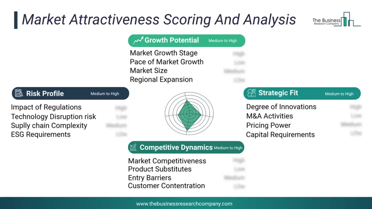
This chart presents market attractiveness based on a quantitative evaluation of growth, competition, strategic alignment, and risk, offering a clear view of opportunity areas for decision-making. This chart is for illustrative purposes; the full report contains the complete analysis.
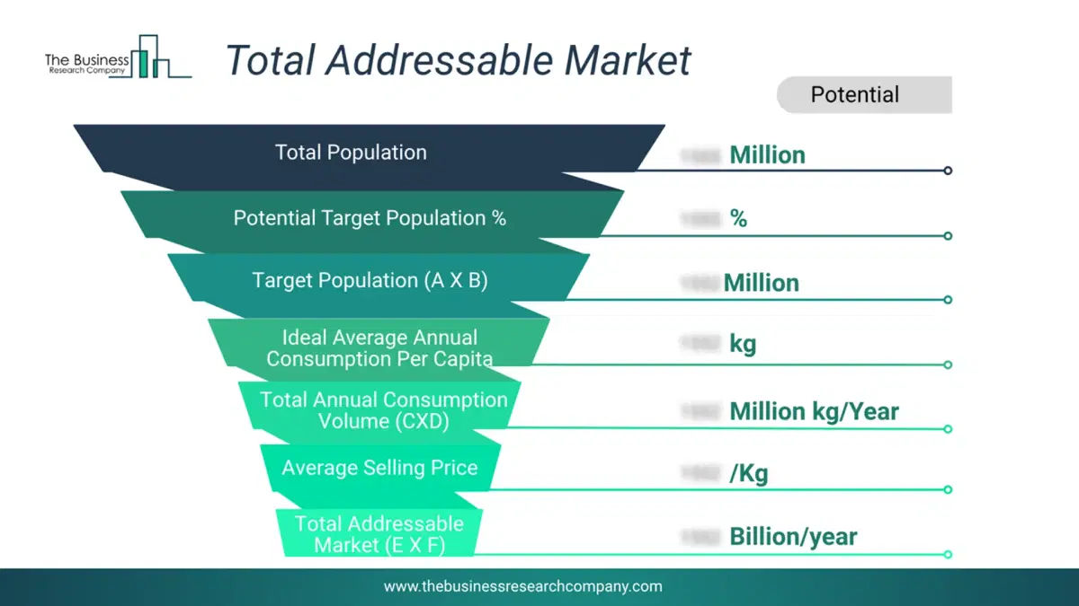
This chart highlights the Total Addressable Market (TAM) by estimating the maximum revenue opportunity using an assumption-driven approach, supporting strategic planning and opportunity sizing across markets. The chart is illustrative; the full report provides a more comprehensive analysis.
What Key Data and Analysis Are Included in the Silicon EPI Wafer Market Report 2026?
The silicon epi wafer market research report is one of a series of new reports from The Business Research Company that provides market statistics, including industry global market size, regional shares, competitors with the market share, detailed market segments, market trends and opportunities, and any further data you may need to thrive in the silicon epi wafer industry. The market research report delivers a complete perspective of everything you need, with an in-depth analysis of the current and future state of the industry.Silicon EPI Wafer Market Report 2026 Market Report Forecast Analysis
| Report Attribute | Details |
|---|---|
| Market Size Value In 2026 | $2 billion |
| Revenue Forecast In 2030 | $2.52 billion |
| Growth Rate | CAGR of 5.9% from 2026 to 2030 |
| Base Year For Estimation | 2025 |
| Actual Estimates/Historical Data | 2020-2025 |
| Forecast Period | 2026 - 2030 |
| Market Representation | Revenue in USD Billion and CAGR from 2026 to 2030 |
| Segments Covered | Type, Equipment, Process Type, Reactors, Industry Vertical |
| Regional Scope | Asia-Pacific, Western Europe, Eastern Europe, North America, South America, Middle East, Africa |
| Country Scope | The countries covered in the report are Australia, Brazil, China, France, Germany, India, Indonesia, Japan, Taiwan, Russia, South Korea, UK, USA, Canada, Italy, Spain. |
| Key Companies Profiled | Shin-Etsu Chemical Co. Ltd., Siltronic AG, GlobalWafers Co. Ltd., SK Siltron Co. Ltd., Okmetic Oy, Sino-American Silicon Products Inc. (SAS), Wafer Works Corporation, Episil-Precision Inc., ShanghAI Simgui Technology Co. Ltd., Soitec SA, IQE PLC, EpiGaN nv, SweGaN AB, Nichia Corporation, AXT Inc., Zhonghuan Semiconductor, LG Siltron Inc., SUMCO Corporation, Mospec Semiconductor Corporation, Komatsu Electronic Materials |
| Customization Scope | Request for Customization |
| Pricing And Purchase Options | Explore Purchase Options |